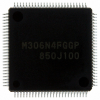
M306N4FGGP#U3 Renesas Electronics America, M306N4FGGP#U3 Datasheet - Page 107

M306N4FGGP#U3
Manufacturer Part Number
M306N4FGGP#U3
Description
IC M16C/6N4 MCU FLASH 100-LQFP
Manufacturer
Renesas Electronics America
Series
M16C™ M16C/6Nr
Specifications of M306N4FGGP#U3
Core Processor
M16C/60
Core Size
16-Bit
Speed
24MHz
Connectivity
CAN, I²C, IEBus, SIO, UART/USART
Peripherals
DMA, WDT
Number Of I /o
85
Program Memory Size
256KB (256K x 8)
Program Memory Type
FLASH
Ram Size
10K x 8
Voltage - Supply (vcc/vdd)
3 V ~ 5.5 V
Data Converters
A/D 26x10b; D/A 2x8b
Oscillator Type
Internal
Operating Temperature
-40°C ~ 85°C
Package / Case
100-LQFP
Package
100LQFP
Family Name
M16C
Maximum Speed
24 MHz
Operating Supply Voltage
3.3|5 V
Data Bus Width
16|32 Bit
Number Of Programmable I/os
87
Interface Type
I2C/UART
On-chip Adc
26-chx10-bit
On-chip Dac
2-chx8-bit
Number Of Timers
11
For Use With
R0K3306NKS001BE - KIT DEV RSK RSK-M16C/6NKR0K3306NKS000BE - KIT DEV RSK RSK-M16C/6NK
Lead Free Status / RoHS Status
Lead free / RoHS Compliant
Eeprom Size
-
Available stocks
Company
Part Number
Manufacturer
Quantity
Price
- Current page: 107 of 414
- Download datasheet (3Mb)
M16C/6N Group (M16C/6N4)
Rev.2.40
REJ09B0009-0240
Figure 10.5 Time Required for Executing Interrupt Sequence
10.5.4 Interrupt Sequence
An interrupt sequence — what are performed over a period from the instant an interrupt is accepted to the
instant the interrupt routine is executed — is described here.
If an interrupt request is generated while an instruction is being executing, the CPU determines its priority
when the execution of the instruction is completed, and transfers control to the interrupt sequence from
the next cycle. However, for the SMOVB, SMOVF, SSTR or RMPA instruction, if an interrupt request is
generated while the instruction is being executing, the MCU temporarily suspends the instruction being
executed, and transfers control to the interrupt sequence.
The CPU behavior during the interrupt sequence is described below.
Figure 10.5 shows the Time Required for Executing Interrupt Sequence.
(1) The CPU obtains interrupt information (interrupt number and interrupt request level) by reading
(2) The FLG register, prior to an interrupt sequence, is saved to a temporary register
(3) Flags I, D, and U in the FLG register become as follows:
(4) The temporary register
(5) The PC is saved to the stack.
(6) The interrupt priority level of the acknowledged interrupt in IPL is set.
(7) The start address of the relevant interrupt routine set in the interrupt vector is stored in the PC.
After the interrupt sequence is completed, an instruction is executed from the starting address of the
interrupt routine.
NOTE:
Address bus
NOTES:
1. The undefined state depends on the instruction queue buffer.
2. The WR signal timing shown here is for the case where the stack is located in the internal RAM.
1. This register cannot be accessed by user.
CPU clock
address 000000h. Then, the IR bit applicable to the interrupt information is set to 0 (interrupt
requested).
• The I flag is set to 0 (interrupt disabled)
• The D flag is set to 0 (single-step interrupt disabled)
• The U flag is set to 0 (ISP selected)
However, the U flag does not change state if an INT instruction for software interrupt Nos. 32 to 63 is
executed.
Apr 14, 2006
Data bus
A read cycle occurs when the instruction queue buffer is ready to accept instructions.
WR
RD
(2)
1
page 83 of 376
Address
0000h
information
2
Interrupt
3
(1)
within the CPU is saved to the stack.
4
Undefined
Undefined
5
Undefined
6
(1)
(1)
7
(1)
8
SP-2
9
contents
SP-2
10
SP-4
11
contents
SP-4
12
13
vec
contents
vec
14
vec+2
15
contents
vec+2
(1)
within the CPU.
16
17
PC
10. Interrupts
18
Related parts for M306N4FGGP#U3
Image
Part Number
Description
Manufacturer
Datasheet
Request
R

Part Number:
Description:
KIT STARTER FOR M16C/29
Manufacturer:
Renesas Electronics America
Datasheet:

Part Number:
Description:
KIT STARTER FOR R8C/2D
Manufacturer:
Renesas Electronics America
Datasheet:

Part Number:
Description:
R0K33062P STARTER KIT
Manufacturer:
Renesas Electronics America
Datasheet:

Part Number:
Description:
KIT STARTER FOR R8C/23 E8A
Manufacturer:
Renesas Electronics America
Datasheet:

Part Number:
Description:
KIT STARTER FOR R8C/25
Manufacturer:
Renesas Electronics America
Datasheet:

Part Number:
Description:
KIT STARTER H8S2456 SHARPE DSPLY
Manufacturer:
Renesas Electronics America
Datasheet:

Part Number:
Description:
KIT STARTER FOR R8C38C
Manufacturer:
Renesas Electronics America
Datasheet:

Part Number:
Description:
KIT STARTER FOR R8C35C
Manufacturer:
Renesas Electronics America
Datasheet:

Part Number:
Description:
KIT STARTER FOR R8CL3AC+LCD APPS
Manufacturer:
Renesas Electronics America
Datasheet:

Part Number:
Description:
KIT STARTER FOR RX610
Manufacturer:
Renesas Electronics America
Datasheet:

Part Number:
Description:
KIT STARTER FOR R32C/118
Manufacturer:
Renesas Electronics America
Datasheet:

Part Number:
Description:
KIT DEV RSK-R8C/26-29
Manufacturer:
Renesas Electronics America
Datasheet:

Part Number:
Description:
KIT STARTER FOR SH7124
Manufacturer:
Renesas Electronics America
Datasheet:

Part Number:
Description:
KIT STARTER FOR H8SX/1622
Manufacturer:
Renesas Electronics America
Datasheet:

Part Number:
Description:
KIT DEV FOR SH7203
Manufacturer:
Renesas Electronics America
Datasheet:


