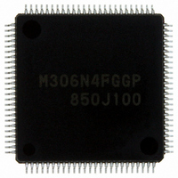
M306N4FGGP#U3 Renesas Electronics America, M306N4FGGP#U3 Datasheet - Page 411

M306N4FGGP#U3
Manufacturer Part Number
M306N4FGGP#U3
Description
IC M16C/6N4 MCU FLASH 100-LQFP
Manufacturer
Renesas Electronics America
Series
M16C™ M16C/6Nr
Specifications of M306N4FGGP#U3
Core Processor
M16C/60
Core Size
16-Bit
Speed
24MHz
Connectivity
CAN, I²C, IEBus, SIO, UART/USART
Peripherals
DMA, WDT
Number Of I /o
85
Program Memory Size
256KB (256K x 8)
Program Memory Type
FLASH
Ram Size
10K x 8
Voltage - Supply (vcc/vdd)
3 V ~ 5.5 V
Data Converters
A/D 26x10b; D/A 2x8b
Oscillator Type
Internal
Operating Temperature
-40°C ~ 85°C
Package / Case
100-LQFP
Package
100LQFP
Family Name
M16C
Maximum Speed
24 MHz
Operating Supply Voltage
3.3|5 V
Data Bus Width
16|32 Bit
Number Of Programmable I/os
87
Interface Type
I2C/UART
On-chip Adc
26-chx10-bit
On-chip Dac
2-chx8-bit
Number Of Timers
11
For Use With
R0K3306NKS001BE - KIT DEV RSK RSK-M16C/6NKR0K3306NKS000BE - KIT DEV RSK RSK-M16C/6NK
Lead Free Status / RoHS Status
Lead free / RoHS Compliant
Eeprom Size
-
Available stocks
Company
Part Number
Manufacturer
Quantity
Price
- Current page: 411 of 414
- Download datasheet (3Mb)
2.40 Apr.14, 2006
Rev.
Date
REVISION HISTORY
142, 143 Figures 15.1 to 15.3 are revised.
Page
111
118
120
125
128
133
134
138
145
146
151
154
159
162
163
167
169
176
183
185
187
189
190
191
192
211
220
224
225
Figure 13.7 Registers TA0MR to TA4MR in Timer Mode: Note 2 is added.
Figure 13.11 Registers TA0MR to TA4MR in One-shot Timer Mode: Note 3 is added.
Figure 13.12 Registers TA0MR to TA4MR in PWM Mode: Note 4 is added.
Figure 13.18 Registers TB0MR to TB5MR in Timer Mode: Note 1 is added.
Figure 13.20 Registers TA0MR to TA4MR in Pulse Period and Pulse Width Measurement
Figure 14.3 INVC1 Register: Note 6 is added.
Figure 14.4 Registers IDB0 and IDB1 (upper): The value of After Reset is revised.
Figure 14.8 Registers TA1MR, TA2MR, TA4MR (upper): Note 1 is added.
Figure 14.8 TB2MR Register (lower): Note 1 is added.
Figure 15.5 Registers U0RB to U2RB (middle): Note 3 is added.
Figure 15.6 Registers U0C0 to U2C0 (lower): Note 6 is added.
Table 15.1 Clock Synchronous Serial I/O Mode Specifications
Figure 15.11 Transmit and Receive Operation is revised.
Table 15.5 UART Mode Specifications
Figure 15.17 Transmit Operation is revised.
Table 15.9 Example of Bit Rates and Settings: “Actual Time” is revised to “Bit Rate”.
Table 15.10 I
Table 15.11 Registers to Be Used and Settings in I
Table 15.14 Special Mode 2 Specifications
Table 15.17 SIM Mode Specifications
Figure 15.32 Transmit and Receive Timing in SIM Mode is revised.
15.1.6.2 Format is revised.
Figure 15.37 S3C Register (upper): Note 6 is added.
Table 15.19 SI/O3 Specifications
Figure 15.38 SI/O3 Operation Timing: Cycle and Note 1 is revised. (1.5 -> 0.5 to 1.0)
15.2.3 Functions for Setting SOUT3 Initial Value: 2nd item (However...) is added.
Figure 17.3 D/A Converter Equivalent Circuit is revised.
Figure 19.7 Registers C0CTLR and C1CTLR (upper): NOTE 4 is added.
Figure 19.11 Registers C0TSR and C1TSR (3rd register): Note 1 is added.
Figure 19.12 Transition between Operational Modes is revised.
• Transfer clock: “fj/2(n+1)” is revised to “fj/(2(n+1))”.
• Note 3 is revised.
• Transfer clock: “fj/16(n+1)” is revised to “fj/(16(n+1))” and “fEXT/16(n+1)” is revised
• Note 2 is revised.
• Transfer clock: “fj/2(n+1)” is revised to “fj/(2(n+1))”.
• Transfer clock: “fj/2(n+1)” is revised to “fj/(2(n+1))”.
• Transfer clock: “fj/16(n+1)” is revised to “fj/(16(n+1))” and “fEXT/16(n+1)” is revised
• Transfer clock: “fj/2(n+1)” is revised to “fj/(2(n+1))”.
Mode: Note 2 is added.
to “fEXT/(16(n+1))” .
to “fEXT/(16(n+1))”.
2
C Mode Specifications
M16C/6N Group (M16C/6N4) Hardware Manual
C-11
Description
Summary
2
C Mode: Note 3 is added.
Related parts for M306N4FGGP#U3
Image
Part Number
Description
Manufacturer
Datasheet
Request
R

Part Number:
Description:
KIT STARTER FOR M16C/29
Manufacturer:
Renesas Electronics America
Datasheet:

Part Number:
Description:
KIT STARTER FOR R8C/2D
Manufacturer:
Renesas Electronics America
Datasheet:

Part Number:
Description:
R0K33062P STARTER KIT
Manufacturer:
Renesas Electronics America
Datasheet:

Part Number:
Description:
KIT STARTER FOR R8C/23 E8A
Manufacturer:
Renesas Electronics America
Datasheet:

Part Number:
Description:
KIT STARTER FOR R8C/25
Manufacturer:
Renesas Electronics America
Datasheet:

Part Number:
Description:
KIT STARTER H8S2456 SHARPE DSPLY
Manufacturer:
Renesas Electronics America
Datasheet:

Part Number:
Description:
KIT STARTER FOR R8C38C
Manufacturer:
Renesas Electronics America
Datasheet:

Part Number:
Description:
KIT STARTER FOR R8C35C
Manufacturer:
Renesas Electronics America
Datasheet:

Part Number:
Description:
KIT STARTER FOR R8CL3AC+LCD APPS
Manufacturer:
Renesas Electronics America
Datasheet:

Part Number:
Description:
KIT STARTER FOR RX610
Manufacturer:
Renesas Electronics America
Datasheet:

Part Number:
Description:
KIT STARTER FOR R32C/118
Manufacturer:
Renesas Electronics America
Datasheet:

Part Number:
Description:
KIT DEV RSK-R8C/26-29
Manufacturer:
Renesas Electronics America
Datasheet:

Part Number:
Description:
KIT STARTER FOR SH7124
Manufacturer:
Renesas Electronics America
Datasheet:

Part Number:
Description:
KIT STARTER FOR H8SX/1622
Manufacturer:
Renesas Electronics America
Datasheet:

Part Number:
Description:
KIT DEV FOR SH7203
Manufacturer:
Renesas Electronics America
Datasheet:


