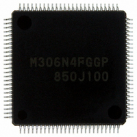
M306N4FGGP#U3 Renesas Electronics America, M306N4FGGP#U3 Datasheet - Page 295

M306N4FGGP#U3
Manufacturer Part Number
M306N4FGGP#U3
Description
IC M16C/6N4 MCU FLASH 100-LQFP
Manufacturer
Renesas Electronics America
Series
M16C™ M16C/6Nr
Specifications of M306N4FGGP#U3
Core Processor
M16C/60
Core Size
16-Bit
Speed
24MHz
Connectivity
CAN, I²C, IEBus, SIO, UART/USART
Peripherals
DMA, WDT
Number Of I /o
85
Program Memory Size
256KB (256K x 8)
Program Memory Type
FLASH
Ram Size
10K x 8
Voltage - Supply (vcc/vdd)
3 V ~ 5.5 V
Data Converters
A/D 26x10b; D/A 2x8b
Oscillator Type
Internal
Operating Temperature
-40°C ~ 85°C
Package / Case
100-LQFP
Package
100LQFP
Family Name
M16C
Maximum Speed
24 MHz
Operating Supply Voltage
3.3|5 V
Data Bus Width
16|32 Bit
Number Of Programmable I/os
87
Interface Type
I2C/UART
On-chip Adc
26-chx10-bit
On-chip Dac
2-chx8-bit
Number Of Timers
11
For Use With
R0K3306NKS001BE - KIT DEV RSK RSK-M16C/6NKR0K3306NKS000BE - KIT DEV RSK RSK-M16C/6NK
Lead Free Status / RoHS Status
Lead free / RoHS Compliant
Eeprom Size
-
Available stocks
Company
Part Number
Manufacturer
Quantity
Price
- Current page: 295 of 414
- Download datasheet (3Mb)
M16C/6N Group (M16C/6N4)
Rev.2.40
REJ09B0009-0240
Table 21.6 Errors and FMR0 Register Status
NOTES:
FMR07 Bit FMR06 Bit
21.3.8 Full Status Check
(SR5)
(Status Register)
If an error occurs when a program or erase operation is completed, the FMR06, FMR07 bits in the FMR0
register are set to 1, indicating a specific error. Therefore, execution results can be confirmed by checking
these bits (full status check).
Table 21.6 lists the Errors and FMR0 Register Status. Figure 21.12 shows a flow chart of the Full Status
Check and Handling Procedure for Each Error.
1. The flash memory enters read array mode by writing command code xxFFh in the second bus cycle of
2. When the FMR02 bit in the FMR0 register is set to 1 (lock bit disabled), no error occurs even under the
FRM00 Register
1
1
0
these commands. The command code written in the first bus cycle becomes invalid.
conditions above.
Apr 14, 2006
Status
(SR4)
1
0
1
page 271 of 376
Command
Sequence
error
Erase error
Program error • The program command is executed on locked blocks
Error
• The lock bit program command is executed but program
• Command is written incorrectly
• A value other than xxD0h or xxFFh is written in the second bus
• The block erase command is executed on a locked block
• The block erase or erase all unlocked block command is
• The program command is executed on unlocked blocks and
operation is not completed as expected
cycle of the lock bit program, block erase or erase all unlocked
block command
executed on an unlock block and auto-erase operation is not
completed as expected
auto-program operation is not completed as expected
Error Occurrence Conditions
(1)
21. Flash Memory Version
(2)
(2)
Related parts for M306N4FGGP#U3
Image
Part Number
Description
Manufacturer
Datasheet
Request
R

Part Number:
Description:
KIT STARTER FOR M16C/29
Manufacturer:
Renesas Electronics America
Datasheet:

Part Number:
Description:
KIT STARTER FOR R8C/2D
Manufacturer:
Renesas Electronics America
Datasheet:

Part Number:
Description:
R0K33062P STARTER KIT
Manufacturer:
Renesas Electronics America
Datasheet:

Part Number:
Description:
KIT STARTER FOR R8C/23 E8A
Manufacturer:
Renesas Electronics America
Datasheet:

Part Number:
Description:
KIT STARTER FOR R8C/25
Manufacturer:
Renesas Electronics America
Datasheet:

Part Number:
Description:
KIT STARTER H8S2456 SHARPE DSPLY
Manufacturer:
Renesas Electronics America
Datasheet:

Part Number:
Description:
KIT STARTER FOR R8C38C
Manufacturer:
Renesas Electronics America
Datasheet:

Part Number:
Description:
KIT STARTER FOR R8C35C
Manufacturer:
Renesas Electronics America
Datasheet:

Part Number:
Description:
KIT STARTER FOR R8CL3AC+LCD APPS
Manufacturer:
Renesas Electronics America
Datasheet:

Part Number:
Description:
KIT STARTER FOR RX610
Manufacturer:
Renesas Electronics America
Datasheet:

Part Number:
Description:
KIT STARTER FOR R32C/118
Manufacturer:
Renesas Electronics America
Datasheet:

Part Number:
Description:
KIT DEV RSK-R8C/26-29
Manufacturer:
Renesas Electronics America
Datasheet:

Part Number:
Description:
KIT STARTER FOR SH7124
Manufacturer:
Renesas Electronics America
Datasheet:

Part Number:
Description:
KIT STARTER FOR H8SX/1622
Manufacturer:
Renesas Electronics America
Datasheet:

Part Number:
Description:
KIT DEV FOR SH7203
Manufacturer:
Renesas Electronics America
Datasheet:


