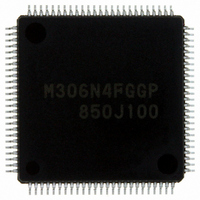
M306N4FGGP#U3 Renesas Electronics America, M306N4FGGP#U3 Datasheet - Page 385

M306N4FGGP#U3
Manufacturer Part Number
M306N4FGGP#U3
Description
IC M16C/6N4 MCU FLASH 100-LQFP
Manufacturer
Renesas Electronics America
Series
M16C™ M16C/6Nr
Specifications of M306N4FGGP#U3
Core Processor
M16C/60
Core Size
16-Bit
Speed
24MHz
Connectivity
CAN, I²C, IEBus, SIO, UART/USART
Peripherals
DMA, WDT
Number Of I /o
85
Program Memory Size
256KB (256K x 8)
Program Memory Type
FLASH
Ram Size
10K x 8
Voltage - Supply (vcc/vdd)
3 V ~ 5.5 V
Data Converters
A/D 26x10b; D/A 2x8b
Oscillator Type
Internal
Operating Temperature
-40°C ~ 85°C
Package / Case
100-LQFP
Package
100LQFP
Family Name
M16C
Maximum Speed
24 MHz
Operating Supply Voltage
3.3|5 V
Data Bus Width
16|32 Bit
Number Of Programmable I/os
87
Interface Type
I2C/UART
On-chip Adc
26-chx10-bit
On-chip Dac
2-chx8-bit
Number Of Timers
11
For Use With
R0K3306NKS001BE - KIT DEV RSK RSK-M16C/6NKR0K3306NKS000BE - KIT DEV RSK RSK-M16C/6NK
Lead Free Status / RoHS Status
Lead free / RoHS Compliant
Eeprom Size
-
Available stocks
Company
Part Number
Manufacturer
Quantity
Price
- Current page: 385 of 414
- Download datasheet (3Mb)
M16C/6N Group (M16C/6N4)
Rev.2.40
REJ09B0009-0240
If the CPU reads the ADi register (i = 0, 1) at the same time the conversion result is stored in the ADi register
after completion of A/D conversion, an incorrect value may be stored in the ADi register. This problem
occurs when a divide-by-n clock derived from the main clock or a sub clock is selected for CPU clock.
• When operating in one-shot or single-sweep mode
• When operating in repeat mode or repeat sweep mode 0 or 1
If A/D conversion is forcibly terminated while in progress by setting the ADST bit in the ADCON0 register to
0 (A/D conversion halted), the conversion result of the A/D converter is undefined. The contents of ADi
register irrelevant to A/D conversion may also become undefined. If while A/D conversion is underway the
ADST bit is set to 0 in a program, ignore the values of all ADi registers.
When setting the ADST bit to 0 in single sweep mode during A/D conversion and A/D conversion is aborted,
disable the interrupt before setting the ADST bit to 0.
The applied intermediate potential may cause more increase in power consumption than other analog input
pins (AN0 to AN3, AN0_0 to AN0_7, and AN2_0 to AN2_7), since the AN4 to AN7 are used with the KI0 to
______
KI3.
Check to see that A/D conversion is completed before reading the target ADi register. (Check the IR bit in
the ADIC register to see if A/D conversion is completed.)
Use the main clock for CPU clock directly without dividing it.
Apr 14, 2006
page 361 of 376
23. Usage Notes
______
Related parts for M306N4FGGP#U3
Image
Part Number
Description
Manufacturer
Datasheet
Request
R

Part Number:
Description:
KIT STARTER FOR M16C/29
Manufacturer:
Renesas Electronics America
Datasheet:

Part Number:
Description:
KIT STARTER FOR R8C/2D
Manufacturer:
Renesas Electronics America
Datasheet:

Part Number:
Description:
R0K33062P STARTER KIT
Manufacturer:
Renesas Electronics America
Datasheet:

Part Number:
Description:
KIT STARTER FOR R8C/23 E8A
Manufacturer:
Renesas Electronics America
Datasheet:

Part Number:
Description:
KIT STARTER FOR R8C/25
Manufacturer:
Renesas Electronics America
Datasheet:

Part Number:
Description:
KIT STARTER H8S2456 SHARPE DSPLY
Manufacturer:
Renesas Electronics America
Datasheet:

Part Number:
Description:
KIT STARTER FOR R8C38C
Manufacturer:
Renesas Electronics America
Datasheet:

Part Number:
Description:
KIT STARTER FOR R8C35C
Manufacturer:
Renesas Electronics America
Datasheet:

Part Number:
Description:
KIT STARTER FOR R8CL3AC+LCD APPS
Manufacturer:
Renesas Electronics America
Datasheet:

Part Number:
Description:
KIT STARTER FOR RX610
Manufacturer:
Renesas Electronics America
Datasheet:

Part Number:
Description:
KIT STARTER FOR R32C/118
Manufacturer:
Renesas Electronics America
Datasheet:

Part Number:
Description:
KIT DEV RSK-R8C/26-29
Manufacturer:
Renesas Electronics America
Datasheet:

Part Number:
Description:
KIT STARTER FOR SH7124
Manufacturer:
Renesas Electronics America
Datasheet:

Part Number:
Description:
KIT STARTER FOR H8SX/1622
Manufacturer:
Renesas Electronics America
Datasheet:

Part Number:
Description:
KIT DEV FOR SH7203
Manufacturer:
Renesas Electronics America
Datasheet:


