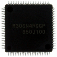
M306N4FGGP#U3 Renesas Electronics America, M306N4FGGP#U3 Datasheet - Page 82

M306N4FGGP#U3
Manufacturer Part Number
M306N4FGGP#U3
Description
IC M16C/6N4 MCU FLASH 100-LQFP
Manufacturer
Renesas Electronics America
Series
M16C™ M16C/6Nr
Specifications of M306N4FGGP#U3
Core Processor
M16C/60
Core Size
16-Bit
Speed
24MHz
Connectivity
CAN, I²C, IEBus, SIO, UART/USART
Peripherals
DMA, WDT
Number Of I /o
85
Program Memory Size
256KB (256K x 8)
Program Memory Type
FLASH
Ram Size
10K x 8
Voltage - Supply (vcc/vdd)
3 V ~ 5.5 V
Data Converters
A/D 26x10b; D/A 2x8b
Oscillator Type
Internal
Operating Temperature
-40°C ~ 85°C
Package / Case
100-LQFP
Package
100LQFP
Family Name
M16C
Maximum Speed
24 MHz
Operating Supply Voltage
3.3|5 V
Data Bus Width
16|32 Bit
Number Of Programmable I/os
87
Interface Type
I2C/UART
On-chip Adc
26-chx10-bit
On-chip Dac
2-chx8-bit
Number Of Timers
11
For Use With
R0K3306NKS001BE - KIT DEV RSK RSK-M16C/6NKR0K3306NKS000BE - KIT DEV RSK RSK-M16C/6NK
Lead Free Status / RoHS Status
Lead free / RoHS Compliant
Eeprom Size
-
Available stocks
Company
Part Number
Manufacturer
Quantity
Price
- Current page: 82 of 414
- Download datasheet (3Mb)
M16C/6N Group (M16C/6N4)
Rev.2.40
REJ09B0009-0240
Figure 8.9 Examples of Main Clock Connection Circuit
The following describes the clocks generated by the clock generation circuit.
8.1.1 Main Clock
The main clock is generated by the main clock oscillation circuit. This clock is used as the clock source for
the CPU and peripheral function clocks. The main clock oscillation circuit is configured by connecting a
resonator between pins XIN and XOUT. The main clock oscillation circuit has an on-chip feedback resistor,
which is disconnected from the oscillation circuit during stop mode in order to reduce the amount of power
consumed in the chip. The main clock oscillation circuit may also be configured by feeding an externally
generated clock to the XIN pin. Figure 8.9 shows an Examples of Main Clock Connection Circuit.
After reset, the main clock divided by 8 is selected for the CPU clock.
The power consumption in the chip can be reduced by setting the CM05 bit in the CM0 register to 1 (main
clock oscillation circuit turned off) after switching the clock source for the CPU clock to a sub clock or on-chip
oscillator clock. In this case, XOUT goes “H”. Furthermore, because an on-chip feedback resistor remains
on, XIN is pulled “H” to XOUT via the feedback resistor. Note, that if an externally generated clock is fed
into the XIN pin, the main clock cannot be turned off by setting the CM05 bit to 1, unless the sub clock is
selected as a CPU clock. If necessary, use an external circuit to turn off the clock.
During stop mode, all clocks including the main clock are turned off. Refer to 8.4 Power Control.
(On-chip feedback resistor)
Apr 14, 2006
NOTE:
1.Place a damping resistor if required. The resistance will vary depending on the oscillator
and the oscillation drive capacity setting. Use the value recommended by each oscillator
the oscillator manufacturer.
When the oscillation drive capacity is set to low, check that oscillation is stable.
Also, place a feedback resistor between XIN and XOUT if the oscillator manufacturer
recommends placing the resistor externally.
MCU
XOUT
page 58 of 376
VSS
XIN
Oscillator
Rd
(1)
COUT
CIN
(On-chip feedback resistor)
MCU
XOUT
XIN
Open
VCC
VSS
External clock
8. Clock Generation Circuit
Related parts for M306N4FGGP#U3
Image
Part Number
Description
Manufacturer
Datasheet
Request
R

Part Number:
Description:
KIT STARTER FOR M16C/29
Manufacturer:
Renesas Electronics America
Datasheet:

Part Number:
Description:
KIT STARTER FOR R8C/2D
Manufacturer:
Renesas Electronics America
Datasheet:

Part Number:
Description:
R0K33062P STARTER KIT
Manufacturer:
Renesas Electronics America
Datasheet:

Part Number:
Description:
KIT STARTER FOR R8C/23 E8A
Manufacturer:
Renesas Electronics America
Datasheet:

Part Number:
Description:
KIT STARTER FOR R8C/25
Manufacturer:
Renesas Electronics America
Datasheet:

Part Number:
Description:
KIT STARTER H8S2456 SHARPE DSPLY
Manufacturer:
Renesas Electronics America
Datasheet:

Part Number:
Description:
KIT STARTER FOR R8C38C
Manufacturer:
Renesas Electronics America
Datasheet:

Part Number:
Description:
KIT STARTER FOR R8C35C
Manufacturer:
Renesas Electronics America
Datasheet:

Part Number:
Description:
KIT STARTER FOR R8CL3AC+LCD APPS
Manufacturer:
Renesas Electronics America
Datasheet:

Part Number:
Description:
KIT STARTER FOR RX610
Manufacturer:
Renesas Electronics America
Datasheet:

Part Number:
Description:
KIT STARTER FOR R32C/118
Manufacturer:
Renesas Electronics America
Datasheet:

Part Number:
Description:
KIT DEV RSK-R8C/26-29
Manufacturer:
Renesas Electronics America
Datasheet:

Part Number:
Description:
KIT STARTER FOR SH7124
Manufacturer:
Renesas Electronics America
Datasheet:

Part Number:
Description:
KIT STARTER FOR H8SX/1622
Manufacturer:
Renesas Electronics America
Datasheet:

Part Number:
Description:
KIT DEV FOR SH7203
Manufacturer:
Renesas Electronics America
Datasheet:


