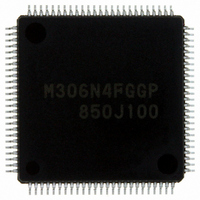
M306N4FGGP#U3 Renesas Electronics America, M306N4FGGP#U3 Datasheet - Page 232

M306N4FGGP#U3
Manufacturer Part Number
M306N4FGGP#U3
Description
IC M16C/6N4 MCU FLASH 100-LQFP
Manufacturer
Renesas Electronics America
Series
M16C™ M16C/6Nr
Specifications of M306N4FGGP#U3
Core Processor
M16C/60
Core Size
16-Bit
Speed
24MHz
Connectivity
CAN, I²C, IEBus, SIO, UART/USART
Peripherals
DMA, WDT
Number Of I /o
85
Program Memory Size
256KB (256K x 8)
Program Memory Type
FLASH
Ram Size
10K x 8
Voltage - Supply (vcc/vdd)
3 V ~ 5.5 V
Data Converters
A/D 26x10b; D/A 2x8b
Oscillator Type
Internal
Operating Temperature
-40°C ~ 85°C
Package / Case
100-LQFP
Package
100LQFP
Family Name
M16C
Maximum Speed
24 MHz
Operating Supply Voltage
3.3|5 V
Data Bus Width
16|32 Bit
Number Of Programmable I/os
87
Interface Type
I2C/UART
On-chip Adc
26-chx10-bit
On-chip Dac
2-chx8-bit
Number Of Timers
11
For Use With
R0K3306NKS001BE - KIT DEV RSK RSK-M16C/6NKR0K3306NKS000BE - KIT DEV RSK RSK-M16C/6NK
Lead Free Status / RoHS Status
Lead free / RoHS Compliant
Eeprom Size
-
Available stocks
Company
Part Number
Manufacturer
Quantity
Price
- Current page: 232 of 414
- Download datasheet (3Mb)
M16C/6N Group (M16C/6N4)
Rev.2.40
REJ09B0009-0240
16.2.5 Current Consumption Reducing Function
16.2.6 Output Impedance of Sensor under A/D Conversion
When not using the A/D converter, its resistor ladder and reference voltage input pin (VREF) can be
separated using the VCUT bit in the ADCON1 register. When separated, no current will flow from the
VREF pin into the resistor ladder, helping to reduce the power consumption of the chip.
To use the A/D converter, set the VCUT bit to 1 (VREF connected) and then set the ADST bit in the
ADCON0 register to 1 (A/D conversion start). The VCUT and ADST bits cannot be set to 1 at the same time.
Nor can the VCUT bit be set to 0 (VREF unconnected) during A/D conversion.
Note that this does not affect VREF for the D/A converter (irrelevant).
To carry out A/D conversion properly, charging the internal capacitor C shown in Figure 16.10 has to be
completed within a specified period of time. T (sampling time) as the specified time. Let output impedance
of sensor equivalent circuit be R0, internal resistance of MCU be R, precision (error) of the A/D converter
be X, and the resolution of A/D converter be Y (Y is 1024 in 10-bit mode, and 256 in 8-bit mode).
Figure 16.10 shows the Analog Input Pin and External Sensor Equivalent Circuit.
When the difference between VIN and VC becomes 0.1 LSB, we find impedance R0 when voltage
between pins VC changes from 0 to VIN-(0.1/1024) VIN in time T. (0.1/1024) means that A/D precision
drop due to insufficient capacitor charge is held to 0.1 LSB at time of A/D conversion in 10-bit mode.
Actual error however is the value of absolute precision added to 0.1 LSB.
When f(φAD) = 10 MHz, T = 0.3 µs in the A/D conversion mode with sample & hold. Output impedance R0
for sufficiently charging capacitor C within time T is determined as follows.
Thus, the allowable output impedance of the sensor equivalent circuit, making the precision (error) 0.1
LSB or less, is approximately 13.9 kΩ. maximum.
Apr 14, 2006
VC is generally VC = VIN {1 – e
And when t = T,
Hence, R0 = –
T = 0.3 µs, R = 7.8 kΩ, C = 1.5 pF, X = 0.1, and Y = 1024. Hence,
R0 = –
1.5 ✕ 10
page 208 of 376
0.3 ✕ 10
C • ln
–12
VC=VIN –
e
–
• ln
–
C (R0 + R)
T
-6
C (R0 + R)
X
Y
1024
1
0.1
1
– R
Y
X
–
T = ln
–7.8 ✕10
T
VIN = VIN(1 –
C (R0 + R)
=
1
Y
X
X
Y
3
t
= 13.9 ✕ 10
}
X
Y
)
3
16. A/D Converter
Related parts for M306N4FGGP#U3
Image
Part Number
Description
Manufacturer
Datasheet
Request
R

Part Number:
Description:
KIT STARTER FOR M16C/29
Manufacturer:
Renesas Electronics America
Datasheet:

Part Number:
Description:
KIT STARTER FOR R8C/2D
Manufacturer:
Renesas Electronics America
Datasheet:

Part Number:
Description:
R0K33062P STARTER KIT
Manufacturer:
Renesas Electronics America
Datasheet:

Part Number:
Description:
KIT STARTER FOR R8C/23 E8A
Manufacturer:
Renesas Electronics America
Datasheet:

Part Number:
Description:
KIT STARTER FOR R8C/25
Manufacturer:
Renesas Electronics America
Datasheet:

Part Number:
Description:
KIT STARTER H8S2456 SHARPE DSPLY
Manufacturer:
Renesas Electronics America
Datasheet:

Part Number:
Description:
KIT STARTER FOR R8C38C
Manufacturer:
Renesas Electronics America
Datasheet:

Part Number:
Description:
KIT STARTER FOR R8C35C
Manufacturer:
Renesas Electronics America
Datasheet:

Part Number:
Description:
KIT STARTER FOR R8CL3AC+LCD APPS
Manufacturer:
Renesas Electronics America
Datasheet:

Part Number:
Description:
KIT STARTER FOR RX610
Manufacturer:
Renesas Electronics America
Datasheet:

Part Number:
Description:
KIT STARTER FOR R32C/118
Manufacturer:
Renesas Electronics America
Datasheet:

Part Number:
Description:
KIT DEV RSK-R8C/26-29
Manufacturer:
Renesas Electronics America
Datasheet:

Part Number:
Description:
KIT STARTER FOR SH7124
Manufacturer:
Renesas Electronics America
Datasheet:

Part Number:
Description:
KIT STARTER FOR H8SX/1622
Manufacturer:
Renesas Electronics America
Datasheet:

Part Number:
Description:
KIT DEV FOR SH7203
Manufacturer:
Renesas Electronics America
Datasheet:


