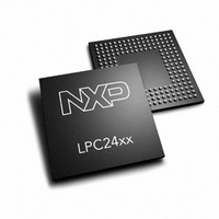
LPC2460FET208,551 NXP Semiconductors, LPC2460FET208,551 Datasheet - Page 376

LPC2460FET208,551
Manufacturer Part Number
LPC2460FET208,551
Description
IC ARM7 MCU ROMLESS 208TFBGA
Manufacturer
NXP Semiconductors
Series
LPC2400r
Specifications of LPC2460FET208,551
Program Memory Type
ROMless
Package / Case
208-TFBGA
Core Processor
ARM7
Core Size
16/32-Bit
Speed
72MHz
Connectivity
CAN, EBI/EMI, Ethernet, I²C, Microwire, MMC, SPI, SSI, SSP, UART/USART, USB OTG
Peripherals
Brown-out Detect/Reset, DMA, I²S, POR, PWM, WDT
Number Of I /o
160
Ram Size
96K x 8
Voltage - Supply (vcc/vdd)
3 V ~ 3.6 V
Data Converters
A/D 8x10b; D/A 1x10b
Oscillator Type
Internal
Operating Temperature
-40°C ~ 85°C
Processor Series
LPC24
Core
ARM7TDMI-S
Data Bus Width
16 bit, 32 bit
Data Ram Size
98 KB
Interface Type
CAN/I2C/I2S/SPI/SSP/UART/USB
Maximum Clock Frequency
72 MHz
Number Of Programmable I/os
160
Number Of Timers
4
Operating Supply Voltage
3.3 V
Maximum Operating Temperature
+ 85 C
Mounting Style
SMD/SMT
3rd Party Development Tools
MDK-ARM, RL-ARM, ULINK2, MCB2460, MCB2460U
Minimum Operating Temperature
- 40 C
On-chip Adc
8-ch x 10-bit
On-chip Dac
1-ch x 10-bit
Lead Free Status / RoHS Status
Lead free / RoHS Compliant
For Use With
MCB2400U - BOARD EVAL MCB2400 + ULINK2MCB2400 - BOARD EVAL FOR NXP LPC246X SER
Eeprom Size
-
Program Memory Size
-
Lead Free Status / Rohs Status
Lead free / RoHS Compliant
Other names
568-4260
935283232551
LPC2460FET208-S
935283232551
LPC2460FET208-S
Available stocks
Company
Part Number
Manufacturer
Quantity
Price
Company:
Part Number:
LPC2460FET208,551
Manufacturer:
NXP Semiconductors
Quantity:
10 000
- Current page: 376 of 792
- Download datasheet (5Mb)
NXP Semiconductors
UM10237_4
User manual
14.4 The DMA descriptor
In DMA mode, the bits corresponding to Interrupt on NAK for Bulk OUT and Interrupt OUT
endpoints (INAK_BO and INAK_IO) should be set to 0 using the SIE Set Mode command
(Section
DMA transfers are described by a data structure called the DMA Descriptor (DD).
DDs are placed in the USB RAM. These descriptors can be located anywhere in the USB
RAM at word-aligned addresses. USB RAM is part of the system memory that is used for
the USB purposes. It is located at address 0x7FD0 0000 and is 8 kB in size.
DDs for non-isochronous endpoints are four words long. DDs for isochronous endpoints
are five words long.
The parameters associated with a DMA transfer are:
Table 13–357
Table 357. DMA descriptor
Word
position
0
1
2
•
•
•
•
•
•
The start address of the DMA buffer
The length of the DMA buffer
The start address of the next DMA descriptor
Control information
Count information (number of bytes transferred)
Status information
13–11.3).
Access
(H/W)
R
R
R
-
R
R
R/W
R/W
[1]
lists the DMA descriptor fields.
Access
(S/W)
R/W
R/W
R/W
-
R/W
R/W
R/W
R/W
Rev. 04 — 26 August 2009
Bit
position
31:0
1:0
2
3
4
15:5
31:16
31:0
Description
Next_DD_pointer (USB RAM address)
DMA_mode (00 -Normal; 01 - ATLE)
Next_DD_valid (1 - valid; 0 - invalid)
Reserved
Isochronous_endpoint (1 - isochronous;
0 - non-isochronous)
Max_packet_size
DMA_buffer_length
This value is specified in bytes for non-isochronous
endpoints and in number of packets for isochronous
endpoints.
DMA_buffer_start_addr
Chapter 13: LPC24XX USB device controller
UM10237
© NXP B.V. 2009. All rights reserved.
376 of 792
Related parts for LPC2460FET208,551
Image
Part Number
Description
Manufacturer
Datasheet
Request
R
Part Number:
Description:
Flashless 16-bit/32-bit Micro; Ethernet, Can, Isp/iap, Usb 2.0 Device/host/otg, External Memory Interface
Manufacturer:
NXP Semiconductors
Datasheet:

Part Number:
Description:
MCU, MPU & DSP Development Tools EVAL BOARD FOR NXP LPC246x
Manufacturer:
Keil Tools
Part Number:
Description:
NXP Semiconductors designed the LPC2420/2460 microcontroller around a 16-bit/32-bitARM7TDMI-S CPU core with real-time debug interfaces that include both JTAG andembedded trace
Manufacturer:
NXP Semiconductors
Datasheet:

Part Number:
Description:
NXP Semiconductors designed the LPC2458 microcontroller around a 16-bit/32-bitARM7TDMI-S CPU core with real-time debug interfaces that include both JTAG andembedded trace
Manufacturer:
NXP Semiconductors
Datasheet:
Part Number:
Description:
NXP Semiconductors designed the LPC2468 microcontroller around a 16-bit/32-bitARM7TDMI-S CPU core with real-time debug interfaces that include both JTAG andembedded trace
Manufacturer:
NXP Semiconductors
Datasheet:
Part Number:
Description:
NXP Semiconductors designed the LPC2470 microcontroller, powered by theARM7TDMI-S core, to be a highly integrated microcontroller for a wide range ofapplications that require advanced communications and high quality graphic displays
Manufacturer:
NXP Semiconductors
Datasheet:
Part Number:
Description:
NXP Semiconductors designed the LPC2478 microcontroller, powered by theARM7TDMI-S core, to be a highly integrated microcontroller for a wide range ofapplications that require advanced communications and high quality graphic displays
Manufacturer:
NXP Semiconductors
Datasheet:
Part Number:
Description:
The Philips Semiconductors XA (eXtended Architecture) family of 16-bit single-chip microcontrollers is powerful enough to easily handle the requirements of high performance embedded applications, yet inexpensive enough to compete in the market for hi
Manufacturer:
NXP Semiconductors
Datasheet:
Part Number:
Description:
The XA-S3 device is a member of Philips Semiconductors? XA(eXtended Architecture) family of high performance 16-bitsingle-chip microcontrollers
Manufacturer:
NXP Semiconductors
Datasheet:

Part Number:
Description:
The NXP BlueStreak LH75401/LH75411 family consists of two low-cost 16/32-bit System-on-Chip (SoC) devices
Manufacturer:
NXP Semiconductors
Datasheet:

Part Number:
Description:
The NXP LPC3130/3131 combine an 180 MHz ARM926EJ-S CPU core, high-speed USB2
Manufacturer:
NXP Semiconductors
Datasheet:

Part Number:
Description:
The NXP LPC3141 combine a 270 MHz ARM926EJ-S CPU core, High-speed USB 2
Manufacturer:
NXP Semiconductors

Part Number:
Description:
The NXP LPC3143 combine a 270 MHz ARM926EJ-S CPU core, High-speed USB 2
Manufacturer:
NXP Semiconductors

Part Number:
Description:
The NXP LPC3152 combines an 180 MHz ARM926EJ-S CPU core, High-speed USB 2
Manufacturer:
NXP Semiconductors


