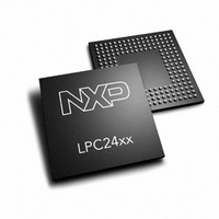
LPC2460FET208,551 NXP Semiconductors, LPC2460FET208,551 Datasheet - Page 674

LPC2460FET208,551
Manufacturer Part Number
LPC2460FET208,551
Description
IC ARM7 MCU ROMLESS 208TFBGA
Manufacturer
NXP Semiconductors
Series
LPC2400r
Specifications of LPC2460FET208,551
Program Memory Type
ROMless
Package / Case
208-TFBGA
Core Processor
ARM7
Core Size
16/32-Bit
Speed
72MHz
Connectivity
CAN, EBI/EMI, Ethernet, I²C, Microwire, MMC, SPI, SSI, SSP, UART/USART, USB OTG
Peripherals
Brown-out Detect/Reset, DMA, I²S, POR, PWM, WDT
Number Of I /o
160
Ram Size
96K x 8
Voltage - Supply (vcc/vdd)
3 V ~ 3.6 V
Data Converters
A/D 8x10b; D/A 1x10b
Oscillator Type
Internal
Operating Temperature
-40°C ~ 85°C
Processor Series
LPC24
Core
ARM7TDMI-S
Data Bus Width
16 bit, 32 bit
Data Ram Size
98 KB
Interface Type
CAN/I2C/I2S/SPI/SSP/UART/USB
Maximum Clock Frequency
72 MHz
Number Of Programmable I/os
160
Number Of Timers
4
Operating Supply Voltage
3.3 V
Maximum Operating Temperature
+ 85 C
Mounting Style
SMD/SMT
3rd Party Development Tools
MDK-ARM, RL-ARM, ULINK2, MCB2460, MCB2460U
Minimum Operating Temperature
- 40 C
On-chip Adc
8-ch x 10-bit
On-chip Dac
1-ch x 10-bit
Lead Free Status / RoHS Status
Lead free / RoHS Compliant
For Use With
MCB2400U - BOARD EVAL MCB2400 + ULINK2MCB2400 - BOARD EVAL FOR NXP LPC246X SER
Eeprom Size
-
Program Memory Size
-
Lead Free Status / Rohs Status
Lead free / RoHS Compliant
Other names
568-4260
935283232551
LPC2460FET208-S
935283232551
LPC2460FET208-S
Available stocks
Company
Part Number
Manufacturer
Quantity
Price
Company:
Part Number:
LPC2460FET208,551
Manufacturer:
NXP Semiconductors
Quantity:
10 000
- Current page: 674 of 792
- Download datasheet (5Mb)
1. Basic configuration
2. Features
3. Pin description
4. Register description (DACR - 0xE006 C000)
UM10237_4
User manual
The DAC is configured using the following registers:
Table 29–598
Table 598. D/A Pin Description
Remark: When the DAC is not used, the V
power supply, and pin V
This read/write register includes the digital value to be converted to analog, and a bit that
trades off performance vs. power. Bits 5:0 are reserved for future, higher-resolution D/A
converters.
Pin
AOUT
VREF
V
1. Power: The DAC is always on.
2. Clock: In the PCLK_SEL0 register
3. Pins: Select the DAC pin and pin mode in registers PINSEL1 and PINMODE1 (see
•
•
•
•
•
DDA
UM10237
Chapter 29: LPC24XX Digital-to Analog Converter (DAC)
Rev. 04 — 26 August 2009
Section
10 bit digital to analog converter
Resistor string architecture
Buffered output
Power-down mode
Selectable speed vs. power
, V
SSA
9–5).
gives a brief summary of each of DAC related pins.
Type
Output
Reference
Power
Rev. 04 — 26 August 2009
SSA
Description
Analog Output. After the selected settling time after the DACR is
written with a new value, the voltage on this pin (with respect to
V
Voltage Reference. This pin provides a voltage reference level for
the D/A converter.
Analog Power and Ground. These should be nominally the same
voltages as V
noise and error.
must be grounded. These pins should not be left floating.
SSA
) is VALUE/1024 × VREF.
(Table
DD(3V3)
DDA
4–56), select PCLK_DAC.
and V
and VREF pins must be connected to the
SS
, but should be isolated to minimize
© NXP B.V. 2009. All rights reserved.
User manual
674 of 792
Related parts for LPC2460FET208,551
Image
Part Number
Description
Manufacturer
Datasheet
Request
R
Part Number:
Description:
Flashless 16-bit/32-bit Micro; Ethernet, Can, Isp/iap, Usb 2.0 Device/host/otg, External Memory Interface
Manufacturer:
NXP Semiconductors
Datasheet:

Part Number:
Description:
MCU, MPU & DSP Development Tools EVAL BOARD FOR NXP LPC246x
Manufacturer:
Keil Tools
Part Number:
Description:
NXP Semiconductors designed the LPC2420/2460 microcontroller around a 16-bit/32-bitARM7TDMI-S CPU core with real-time debug interfaces that include both JTAG andembedded trace
Manufacturer:
NXP Semiconductors
Datasheet:

Part Number:
Description:
NXP Semiconductors designed the LPC2458 microcontroller around a 16-bit/32-bitARM7TDMI-S CPU core with real-time debug interfaces that include both JTAG andembedded trace
Manufacturer:
NXP Semiconductors
Datasheet:
Part Number:
Description:
NXP Semiconductors designed the LPC2468 microcontroller around a 16-bit/32-bitARM7TDMI-S CPU core with real-time debug interfaces that include both JTAG andembedded trace
Manufacturer:
NXP Semiconductors
Datasheet:
Part Number:
Description:
NXP Semiconductors designed the LPC2470 microcontroller, powered by theARM7TDMI-S core, to be a highly integrated microcontroller for a wide range ofapplications that require advanced communications and high quality graphic displays
Manufacturer:
NXP Semiconductors
Datasheet:
Part Number:
Description:
NXP Semiconductors designed the LPC2478 microcontroller, powered by theARM7TDMI-S core, to be a highly integrated microcontroller for a wide range ofapplications that require advanced communications and high quality graphic displays
Manufacturer:
NXP Semiconductors
Datasheet:
Part Number:
Description:
The Philips Semiconductors XA (eXtended Architecture) family of 16-bit single-chip microcontrollers is powerful enough to easily handle the requirements of high performance embedded applications, yet inexpensive enough to compete in the market for hi
Manufacturer:
NXP Semiconductors
Datasheet:
Part Number:
Description:
The XA-S3 device is a member of Philips Semiconductors? XA(eXtended Architecture) family of high performance 16-bitsingle-chip microcontrollers
Manufacturer:
NXP Semiconductors
Datasheet:

Part Number:
Description:
The NXP BlueStreak LH75401/LH75411 family consists of two low-cost 16/32-bit System-on-Chip (SoC) devices
Manufacturer:
NXP Semiconductors
Datasheet:

Part Number:
Description:
The NXP LPC3130/3131 combine an 180 MHz ARM926EJ-S CPU core, high-speed USB2
Manufacturer:
NXP Semiconductors
Datasheet:

Part Number:
Description:
The NXP LPC3141 combine a 270 MHz ARM926EJ-S CPU core, High-speed USB 2
Manufacturer:
NXP Semiconductors

Part Number:
Description:
The NXP LPC3143 combine a 270 MHz ARM926EJ-S CPU core, High-speed USB 2
Manufacturer:
NXP Semiconductors

Part Number:
Description:
The NXP LPC3152 combines an 180 MHz ARM926EJ-S CPU core, High-speed USB 2
Manufacturer:
NXP Semiconductors


