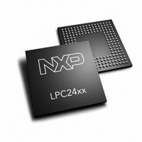
LPC2460FET208,551 NXP Semiconductors, LPC2460FET208,551 Datasheet - Page 698

LPC2460FET208,551
Manufacturer Part Number
LPC2460FET208,551
Description
IC ARM7 MCU ROMLESS 208TFBGA
Manufacturer
NXP Semiconductors
Series
LPC2400r
Specifications of LPC2460FET208,551
Program Memory Type
ROMless
Package / Case
208-TFBGA
Core Processor
ARM7
Core Size
16/32-Bit
Speed
72MHz
Connectivity
CAN, EBI/EMI, Ethernet, I²C, Microwire, MMC, SPI, SSI, SSP, UART/USART, USB OTG
Peripherals
Brown-out Detect/Reset, DMA, I²S, POR, PWM, WDT
Number Of I /o
160
Ram Size
96K x 8
Voltage - Supply (vcc/vdd)
3 V ~ 3.6 V
Data Converters
A/D 8x10b; D/A 1x10b
Oscillator Type
Internal
Operating Temperature
-40°C ~ 85°C
Processor Series
LPC24
Core
ARM7TDMI-S
Data Bus Width
16 bit, 32 bit
Data Ram Size
98 KB
Interface Type
CAN/I2C/I2S/SPI/SSP/UART/USB
Maximum Clock Frequency
72 MHz
Number Of Programmable I/os
160
Number Of Timers
4
Operating Supply Voltage
3.3 V
Maximum Operating Temperature
+ 85 C
Mounting Style
SMD/SMT
3rd Party Development Tools
MDK-ARM, RL-ARM, ULINK2, MCB2460, MCB2460U
Minimum Operating Temperature
- 40 C
On-chip Adc
8-ch x 10-bit
On-chip Dac
1-ch x 10-bit
Lead Free Status / RoHS Status
Lead free / RoHS Compliant
For Use With
MCB2400U - BOARD EVAL MCB2400 + ULINK2MCB2400 - BOARD EVAL FOR NXP LPC246X SER
Eeprom Size
-
Program Memory Size
-
Lead Free Status / Rohs Status
Lead free / RoHS Compliant
Other names
568-4260
935283232551
LPC2460FET208-S
935283232551
LPC2460FET208-S
Available stocks
Company
Part Number
Manufacturer
Quantity
Price
Company:
Part Number:
LPC2460FET208,551
Manufacturer:
NXP Semiconductors
Quantity:
10 000
- Current page: 698 of 792
- Download datasheet (5Mb)
NXP Semiconductors
UM10237_4
User manual
4.1 Memory map after any reset
4.2 Communication protocol
Pin P2.10 that is used as hardware request for ISP requires special attention. Since P2.10
is in high impedance mode after reset, it is important that the user provides external
hardware (a pull-up resistor or other device) to put the pin in a defined state. Otherwise
unintended entry into ISP mode may occur.
When ISP mode is entered after a power on reset, the IRC and PLL are used to generate
CCLK of 14.748 MHz.
The boot loader resides in an on-chip ROM sector of 8 kB in size. After any reset the
entire boot sector is also mapped to the top of the on-chip memory space i.e. the boot
block is also visible in the memory region starting from the address 0x7FFF E000. The
serial boot loader is designed to run from this memory area, and both the ISP and IAP
software use parts of the on-chip RAM. The RAM usage is described later in this chapter.
In addition, the bottom 64 byte of the ROM boot sector are also visible in the memory
region starting from address 0x0000 0000, i.e. the interrupt vectors are mapped to the
boot ROM sector. The reset vector contains a jump instruction to the entry point of the
serial boot loader software.
All ISP commands should be sent as single ASCII strings. Strings should be terminated
with Carriage Return (CR) and/or Line Feed (LF) control characters. Extra <CR> and
<LF> characters are ignored. All ISP responses are sent as <CR><LF> terminated ASCII
strings. Data is sent and received in UU-encoded format.
Fig 141. Map of lower memory after reset for flashless LPC2400 parts
2.0 GB - 8 kB
0.0 GB
2.0 GB
Rev. 04 — 26 August 2009
Chapter 31: LPC24XX On-chip bootloader for flashless parts
(BOOT BLOCK INTERRUPT VECTORS)
ACTIVE INTERRUPT VECTORS
FROM THE BOOT BLOCK
8 kB BOOT BLOCK
UM10237
0x7FFF FFFF
0x7FFF E000
0x0000 0000
© NXP B.V. 2009. All rights reserved.
698 of 792
Related parts for LPC2460FET208,551
Image
Part Number
Description
Manufacturer
Datasheet
Request
R
Part Number:
Description:
Flashless 16-bit/32-bit Micro; Ethernet, Can, Isp/iap, Usb 2.0 Device/host/otg, External Memory Interface
Manufacturer:
NXP Semiconductors
Datasheet:

Part Number:
Description:
MCU, MPU & DSP Development Tools EVAL BOARD FOR NXP LPC246x
Manufacturer:
Keil Tools
Part Number:
Description:
NXP Semiconductors designed the LPC2420/2460 microcontroller around a 16-bit/32-bitARM7TDMI-S CPU core with real-time debug interfaces that include both JTAG andembedded trace
Manufacturer:
NXP Semiconductors
Datasheet:

Part Number:
Description:
NXP Semiconductors designed the LPC2458 microcontroller around a 16-bit/32-bitARM7TDMI-S CPU core with real-time debug interfaces that include both JTAG andembedded trace
Manufacturer:
NXP Semiconductors
Datasheet:
Part Number:
Description:
NXP Semiconductors designed the LPC2468 microcontroller around a 16-bit/32-bitARM7TDMI-S CPU core with real-time debug interfaces that include both JTAG andembedded trace
Manufacturer:
NXP Semiconductors
Datasheet:
Part Number:
Description:
NXP Semiconductors designed the LPC2470 microcontroller, powered by theARM7TDMI-S core, to be a highly integrated microcontroller for a wide range ofapplications that require advanced communications and high quality graphic displays
Manufacturer:
NXP Semiconductors
Datasheet:
Part Number:
Description:
NXP Semiconductors designed the LPC2478 microcontroller, powered by theARM7TDMI-S core, to be a highly integrated microcontroller for a wide range ofapplications that require advanced communications and high quality graphic displays
Manufacturer:
NXP Semiconductors
Datasheet:
Part Number:
Description:
The Philips Semiconductors XA (eXtended Architecture) family of 16-bit single-chip microcontrollers is powerful enough to easily handle the requirements of high performance embedded applications, yet inexpensive enough to compete in the market for hi
Manufacturer:
NXP Semiconductors
Datasheet:
Part Number:
Description:
The XA-S3 device is a member of Philips Semiconductors? XA(eXtended Architecture) family of high performance 16-bitsingle-chip microcontrollers
Manufacturer:
NXP Semiconductors
Datasheet:

Part Number:
Description:
The NXP BlueStreak LH75401/LH75411 family consists of two low-cost 16/32-bit System-on-Chip (SoC) devices
Manufacturer:
NXP Semiconductors
Datasheet:

Part Number:
Description:
The NXP LPC3130/3131 combine an 180 MHz ARM926EJ-S CPU core, high-speed USB2
Manufacturer:
NXP Semiconductors
Datasheet:

Part Number:
Description:
The NXP LPC3141 combine a 270 MHz ARM926EJ-S CPU core, High-speed USB 2
Manufacturer:
NXP Semiconductors

Part Number:
Description:
The NXP LPC3143 combine a 270 MHz ARM926EJ-S CPU core, High-speed USB 2
Manufacturer:
NXP Semiconductors

Part Number:
Description:
The NXP LPC3152 combines an 180 MHz ARM926EJ-S CPU core, High-speed USB 2
Manufacturer:
NXP Semiconductors


