EVB9S12XEP100 Freescale Semiconductor, EVB9S12XEP100 Datasheet - Page 209
EVB9S12XEP100
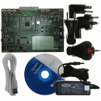
Manufacturer Part Number
EVB9S12XEP100
Description
BOARD EVAL FOR MC9S12XEP100
Manufacturer
Freescale Semiconductor
Type
MCUr
Datasheet
1.EVB9S12XEP100.pdf
(1328 pages)
Specifications of EVB9S12XEP100
Contents
Module and Misc Hardware
Processor To Be Evaluated
MC9S12XEP100
Data Bus Width
16 bit
Interface Type
RS-232
Silicon Manufacturer
Freescale
Core Architecture
S12
Core Sub-architecture
S12
Silicon Core Number
MC9S12
Silicon Family Name
S12XE
Rohs Compliant
Yes
For Use With/related Products
MC9S12XEP100
Lead Free Status / RoHS Status
Lead free / RoHS Compliant


3.4.2
3.4.2.1
The BDM firmware lookup tables and BDM register memory locations share addresses with other
modules; however they are not visible in the memory map during user’s code execution. The BDM
memory resources are enabled only during the READ_BD and WRITE_BD access cycles to distinguish
between accesses to the BDM memory area and accesses to the other modules. (Refer to BDM Block
Guide for further details).
When the MCU enters active BDM mode, the BDM firmware lookup tables and the BDM registers
become visible in the local memory map in the range 0xFF00-0xFFFF (global address 0x7F_FF00 -
0x7F_FFFF) and the CPU begins execution of firmware commands or the BDM begins execution of
hardware commands. The resources which share memory space with the BDM module will not be visible
in the memory map during active BDM mode.
Please note that after the MCU enters active BDM mode the BDM firmware lookup tables and the BDM
registers will also be visible between addresses 0xBF00 and 0xBFFF if the PPAGE register contains value
of 0xFF.
Freescale Semiconductor
Because of an order from the United States International Trade Commission, BGA-packaged product lines and partnumbers
indicated here currently are not available from Freescale for import or sale in the United States prior to September 2010
•
•
•
•
Emulation single-chip mode
Tool vendors use this mode for emulation systems in which the user’s target application is normal
single-chip mode. Code is executed from external or internal memory depending on the set-up of
the EROMON bit (see
is active in both cases to allow observation of internal operations (internal visibility).
Normal expanded mode
The external bus interface is configured as an up to 23-bit address bus, 8 or 16-bit data bus with
dedicated bus control and status signals. This mode allows 8 or 16-bit external memory and
peripheral devices to be interfaced to the system. The fastest external bus rate is half of the internal
bus rate. An external signal can be used in this mode to cause the external bus to wait as desired by
the external logic.
Emulation expanded mode
Tool vendors use this mode for emulation systems in which the user’s target application is normal
expanded mode.
Special test mode
This mode is an expanded mode for factory test.
Memory Map Scheme
CPU and BDM Memory Map Scheme
Section 3.3.2.5, “MMC Control Register
MC9S12XE-Family Reference Manual Rev. 1.23
Chapter 3 Memory Mapping Control (S12XMMCV4)
(MMCCTL1)). The external bus
209
Related parts for EVB9S12XEP100
Image
Part Number
Description
Manufacturer
Datasheet
Request
R

Part Number:
Description:
Manufacturer:
Freescale Semiconductor, Inc
Datasheet:
Part Number:
Description:
Manufacturer:
Freescale Semiconductor, Inc
Datasheet:
Part Number:
Description:
Manufacturer:
Freescale Semiconductor, Inc
Datasheet:
Part Number:
Description:
Manufacturer:
Freescale Semiconductor, Inc
Datasheet:
Part Number:
Description:
Manufacturer:
Freescale Semiconductor, Inc
Datasheet:
Part Number:
Description:
Manufacturer:
Freescale Semiconductor, Inc
Datasheet:
Part Number:
Description:
Manufacturer:
Freescale Semiconductor, Inc
Datasheet:
Part Number:
Description:
Manufacturer:
Freescale Semiconductor, Inc
Datasheet:
Part Number:
Description:
Manufacturer:
Freescale Semiconductor, Inc
Datasheet:
Part Number:
Description:
Manufacturer:
Freescale Semiconductor, Inc
Datasheet:
Part Number:
Description:
Manufacturer:
Freescale Semiconductor, Inc
Datasheet:
Part Number:
Description:
Manufacturer:
Freescale Semiconductor, Inc
Datasheet:
Part Number:
Description:
Manufacturer:
Freescale Semiconductor, Inc
Datasheet:
Part Number:
Description:
Manufacturer:
Freescale Semiconductor, Inc
Datasheet:
Part Number:
Description:
Manufacturer:
Freescale Semiconductor, Inc
Datasheet: