EVB9S12XEP100 Freescale Semiconductor, EVB9S12XEP100 Datasheet - Page 720
EVB9S12XEP100
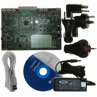
Manufacturer Part Number
EVB9S12XEP100
Description
BOARD EVAL FOR MC9S12XEP100
Manufacturer
Freescale Semiconductor
Type
MCUr
Datasheet
1.EVB9S12XEP100.pdf
(1328 pages)
Specifications of EVB9S12XEP100
Contents
Module and Misc Hardware
Processor To Be Evaluated
MC9S12XEP100
Data Bus Width
16 bit
Interface Type
RS-232
Silicon Manufacturer
Freescale
Core Architecture
S12
Core Sub-architecture
S12
Silicon Core Number
MC9S12
Silicon Family Name
S12XE
Rohs Compliant
Yes
For Use With/related Products
MC9S12XEP100
Lead Free Status / RoHS Status
Lead free / RoHS Compliant


Chapter 19 Pulse-Width Modulator (S12PWM8B8CV1)
As an example of a center aligned output, consider the following case:
Shown in
19.4.2.7
The PWM timer also has the option of generating 8-channels of 8-bits or 4-channels of 16-bits for greater
PWM resolution. This 16-bit channel option is achieved through the concatenation of two 8-bit channels.
The PWMCTL register contains four control bits, each of which is used to concatenate a pair of PWM
channels into one 16-bit channel. Channels 6 and 7 are concatenated with the CON67 bit, channels 4 and
5 are concatenated with the CON45 bit, channels 2 and 3 are concatenated with the CON23 bit, and
channels 0 and 1 are concatenated with the CON01 bit.
When channels 6 and 7 are concatenated, channel 6 registers become the high order bytes of the double
byte channel, as shown in
registers become the high order bytes of the double byte channel. When channels 2 and 3 are concatenated,
channel 2 registers become the high order bytes of the double byte channel. When channels 0 and 1 are
concatenated, channel 0 registers become the high order bytes of the double byte channel.
When using the 16-bit concatenated mode, the clock source is determined by the low order 8-bit channel
clock select control bits. That is channel 7 when channels 6 and 7 are concatenated, channel 5 when
channels 4 and 5 are concatenated, channel 3 when channels 2 and 3 are concatenated, and channel 1 when
channels 0 and 1 are concatenated. The resulting PWM is output to the pins of the corresponding low order
8-bit channel as also shown in
PPOLx bit of the corresponding low order 8-bit channel as well.
720
Because of an order from the United States International Trade Commission, BGA-packaged product lines and partnumbers
indicated here currently are not available from Freescale for import or sale in the United States prior to September 2010
E = 100 ns
Clock Source = E, where E = 10 MHz (100 ns period)
PWMx Frequency = 10 MHz/8 = 1.25 MHz
PWMx Period = 800 ns
PWMx Duty Cycle = 3/4 *100% = 75%
Figure 19-23
PPOLx = 0
PWMPERx = 4
PWMDTYx = 1
PWM 16-Bit Functions
Change these bits only when both corresponding channels are disabled.
Figure 19-23. PWM Center Aligned Output Example Waveform
is the output waveform generated.
Figure
Figure
MC9S12XE-Family Reference Manual , Rev. 1.23
19-24. Similarly, when channels 4 and 5 are concatenated, channel 4
19-24. The polarity of the resulting PWM output is controlled by the
DUTY CYCLE = 75%
PERIOD = 800 ns
NOTE
Freescale Semiconductor
E = 100 ns
Related parts for EVB9S12XEP100
Image
Part Number
Description
Manufacturer
Datasheet
Request
R

Part Number:
Description:
Manufacturer:
Freescale Semiconductor, Inc
Datasheet:
Part Number:
Description:
Manufacturer:
Freescale Semiconductor, Inc
Datasheet:
Part Number:
Description:
Manufacturer:
Freescale Semiconductor, Inc
Datasheet:
Part Number:
Description:
Manufacturer:
Freescale Semiconductor, Inc
Datasheet:
Part Number:
Description:
Manufacturer:
Freescale Semiconductor, Inc
Datasheet:
Part Number:
Description:
Manufacturer:
Freescale Semiconductor, Inc
Datasheet:
Part Number:
Description:
Manufacturer:
Freescale Semiconductor, Inc
Datasheet:
Part Number:
Description:
Manufacturer:
Freescale Semiconductor, Inc
Datasheet:
Part Number:
Description:
Manufacturer:
Freescale Semiconductor, Inc
Datasheet:
Part Number:
Description:
Manufacturer:
Freescale Semiconductor, Inc
Datasheet:
Part Number:
Description:
Manufacturer:
Freescale Semiconductor, Inc
Datasheet:
Part Number:
Description:
Manufacturer:
Freescale Semiconductor, Inc
Datasheet:
Part Number:
Description:
Manufacturer:
Freescale Semiconductor, Inc
Datasheet:
Part Number:
Description:
Manufacturer:
Freescale Semiconductor, Inc
Datasheet:
Part Number:
Description:
Manufacturer:
Freescale Semiconductor, Inc
Datasheet: