EVB9S12XEP100 Freescale Semiconductor, EVB9S12XEP100 Datasheet - Page 711
EVB9S12XEP100
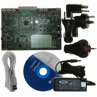
Manufacturer Part Number
EVB9S12XEP100
Description
BOARD EVAL FOR MC9S12XEP100
Manufacturer
Freescale Semiconductor
Type
MCUr
Datasheet
1.EVB9S12XEP100.pdf
(1328 pages)
Specifications of EVB9S12XEP100
Contents
Module and Misc Hardware
Processor To Be Evaluated
MC9S12XEP100
Data Bus Width
16 bit
Interface Type
RS-232
Silicon Manufacturer
Freescale
Core Architecture
S12
Core Sub-architecture
S12
Silicon Core Number
MC9S12
Silicon Family Name
S12XE
Rohs Compliant
Yes
For Use With/related Products
MC9S12XEP100
Lead Free Status / RoHS Status
Lead free / RoHS Compliant


19.4
19.4.1
There are four available clocks: clock A, clock B, clock SA (scaled A), and clock SB (scaled B). These
four clocks are based on the bus clock.
Clock A and B can be software selected to be 1, 1/2, 1/4, 1/8,..., 1/64, 1/128 times the bus clock. Clock SA
uses clock A as an input and divides it further with a reloadable counter. Similarly, clock SB uses clock B
as an input and divides it further with a reloadable counter. The rates available for clock SA are software
selectable to be clock A divided by 2, 4, 6, 8,..., or 512 in increments of divide by 2. Similar rates are
available for clock SB. Each PWM channel has the capability of selecting one of two clocks, either the
pre-scaled clock (clock A or B) or the scaled clock (clock SA or SB).
The block diagram in
19.4.1.1
The input clock to the PWM prescaler is the bus clock. It can be disabled whenever the part is in freeze
mode by setting the PFRZ bit in the PWMCTL register. If this bit is set, whenever the MCU is in freeze
mode (freeze mode signal active) the input clock to the prescaler is disabled. This is useful for emulation
in order to freeze the PWM. The input clock can also be disabled when all eight PWM channels are
disabled (PWME7-0 = 0). This is useful for reducing power by disabling the prescale counter.
Clock A and clock B are scaled values of the input clock. The value is software selectable for both clock
A and clock B and has options of 1, 1/2, 1/4, 1/8, 1/16, 1/32, 1/64, or 1/128 times the bus clock. The value
selected for clock A is determined by the PCKA2, PCKA1, PCKA0 bits in the PWMPRCLK register. The
value selected for clock B is determined by the PCKB2, PCKB1, PCKB0 bits also in the PWMPRCLK
register.
Freescale Semiconductor
PWM7ENA
Because of an order from the United States International Trade Commission, BGA-packaged product lines and partnumbers
PWM7INL
PWMLVL
PWM7IN
indicated here currently are not available from Freescale for import or sale in the United States prior to September 2010
Field
4
2
1
0
Functional Description
PWM Clock Select
PWM Shutdown Output Level If active level as defined by the PWM7IN input, gets asserted all enabled PWM
channels are immediately driven to the level defined by PWMLVL.
0 PWM outputs are forced to 0
1 Outputs are forced to 1.
PWM Channel 7 Input Status — This reflects the current status of the PWM7 pin.
PWM Shutdown Active Input Level for Channel 7 — If the emergency shutdown feature is enabled
(PWM7ENA = 1), this bit determines the active level of the PWM7channel.
0 Active level is low
1 Active level is high
PWM Emergency Shutdown Enable — If this bit is logic 1, the pin associated with channel 7 is forced to input
and the emergency shutdown feature is enabled. All the other bits in this register are meaningful only if
PWM7ENA = 1.
0 PWM emergency feature disabled.
1 PWM emergency feature is enabled.
Prescale
Figure 19-18
MC9S12XE-Family Reference Manual Rev. 1.23
shows the four different clocks and how the scaled clocks are created.
Description
Chapter 19 Pulse-Width Modulator (S12PWM8B8CV1)
711
Related parts for EVB9S12XEP100
Image
Part Number
Description
Manufacturer
Datasheet
Request
R

Part Number:
Description:
Manufacturer:
Freescale Semiconductor, Inc
Datasheet:
Part Number:
Description:
Manufacturer:
Freescale Semiconductor, Inc
Datasheet:
Part Number:
Description:
Manufacturer:
Freescale Semiconductor, Inc
Datasheet:
Part Number:
Description:
Manufacturer:
Freescale Semiconductor, Inc
Datasheet:
Part Number:
Description:
Manufacturer:
Freescale Semiconductor, Inc
Datasheet:
Part Number:
Description:
Manufacturer:
Freescale Semiconductor, Inc
Datasheet:
Part Number:
Description:
Manufacturer:
Freescale Semiconductor, Inc
Datasheet:
Part Number:
Description:
Manufacturer:
Freescale Semiconductor, Inc
Datasheet:
Part Number:
Description:
Manufacturer:
Freescale Semiconductor, Inc
Datasheet:
Part Number:
Description:
Manufacturer:
Freescale Semiconductor, Inc
Datasheet:
Part Number:
Description:
Manufacturer:
Freescale Semiconductor, Inc
Datasheet:
Part Number:
Description:
Manufacturer:
Freescale Semiconductor, Inc
Datasheet:
Part Number:
Description:
Manufacturer:
Freescale Semiconductor, Inc
Datasheet:
Part Number:
Description:
Manufacturer:
Freescale Semiconductor, Inc
Datasheet:
Part Number:
Description:
Manufacturer:
Freescale Semiconductor, Inc
Datasheet: