EVB9S12XEP100 Freescale Semiconductor, EVB9S12XEP100 Datasheet - Page 504
EVB9S12XEP100
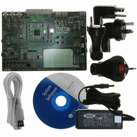
Manufacturer Part Number
EVB9S12XEP100
Description
BOARD EVAL FOR MC9S12XEP100
Manufacturer
Freescale Semiconductor
Type
MCUr
Datasheet
1.EVB9S12XEP100.pdf
(1328 pages)
Specifications of EVB9S12XEP100
Contents
Module and Misc Hardware
Processor To Be Evaluated
MC9S12XEP100
Data Bus Width
16 bit
Interface Type
RS-232
Silicon Manufacturer
Freescale
Core Architecture
S12
Core Sub-architecture
S12
Silicon Core Number
MC9S12
Silicon Family Name
S12XE
Rohs Compliant
Yes
For Use With/related Products
MC9S12XEP100
Lead Free Status / RoHS Status
Lead free / RoHS Compliant


Chapter 12 Pierce Oscillator (S12XOSCLCPV2)
12.3
The CRG contains the registers and associated bits for controlling and monitoring the oscillator module.
12.4
The XOSC module has control circuitry to maintain the crystal oscillator circuit voltage level to an optimal
level which is determined by the amount of hysteresis being used and the maximum oscillation range.
The oscillator block has two external pins, EXTAL and XTAL. The oscillator input pin, EXTAL, is
intended to be connected to either a crystal or an external clock source. The XTAL pin is an output signal
that provides crystal circuit feedback.
A buffered EXTAL signal becomes the internal clock. To improve noise immunity, the oscillator is
powered by the VDDPLL and VSSPLL power supply pins.
12.4.1
In LCP mode a closed loop control system will be utilized whereby the amplifier is modulated to keep the
output waveform sinusoidal and to limit the oscillation amplitude. The output peak to peak voltage will be
kept above twice the maximum hysteresis level of the input buffer. Electrical specification details are
provided in the Electrical Characteristics appendix.
12.4.2
The clock monitor circuit is based on an internal RC time delay so that it can operate without any MCU
clocks. If no OSCCLK edges are detected within this RC time delay, the clock monitor indicates failure
which asserts self-clock mode or generates a system reset depending on the state of SCME bit. If the clock
monitor is disabled or the presence of clocks is detected no failure is indicated.The clock monitor function
is enabled/disabled by the CME control bit, described in the CRG block description chapter.
12.4.3
During wait mode, XOSC is not impacted.
12.4.4
XOSC is placed in a static state when the part is in stop mode except when pseudo-stop mode is enabled.
During pseudo-stop mode, XOSC is not impacted.
504
Because of an order from the United States International Trade Commission, BGA-packaged product lines and partnumbers
indicated here currently are not available from Freescale for import or sale in the United States prior to September 2010
Memory Map and Register Definition
Functional Description
Gain Control
Clock Monitor
Wait Mode Operation
Stop Mode Operation
MC9S12XE-Family Reference Manual , Rev. 1.23
Freescale Semiconductor
Related parts for EVB9S12XEP100
Image
Part Number
Description
Manufacturer
Datasheet
Request
R

Part Number:
Description:
Manufacturer:
Freescale Semiconductor, Inc
Datasheet:
Part Number:
Description:
Manufacturer:
Freescale Semiconductor, Inc
Datasheet:
Part Number:
Description:
Manufacturer:
Freescale Semiconductor, Inc
Datasheet:
Part Number:
Description:
Manufacturer:
Freescale Semiconductor, Inc
Datasheet:
Part Number:
Description:
Manufacturer:
Freescale Semiconductor, Inc
Datasheet:
Part Number:
Description:
Manufacturer:
Freescale Semiconductor, Inc
Datasheet:
Part Number:
Description:
Manufacturer:
Freescale Semiconductor, Inc
Datasheet:
Part Number:
Description:
Manufacturer:
Freescale Semiconductor, Inc
Datasheet:
Part Number:
Description:
Manufacturer:
Freescale Semiconductor, Inc
Datasheet:
Part Number:
Description:
Manufacturer:
Freescale Semiconductor, Inc
Datasheet:
Part Number:
Description:
Manufacturer:
Freescale Semiconductor, Inc
Datasheet:
Part Number:
Description:
Manufacturer:
Freescale Semiconductor, Inc
Datasheet:
Part Number:
Description:
Manufacturer:
Freescale Semiconductor, Inc
Datasheet:
Part Number:
Description:
Manufacturer:
Freescale Semiconductor, Inc
Datasheet:
Part Number:
Description:
Manufacturer:
Freescale Semiconductor, Inc
Datasheet: