EVB9S12XEP100 Freescale Semiconductor, EVB9S12XEP100 Datasheet - Page 71
EVB9S12XEP100
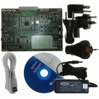
Manufacturer Part Number
EVB9S12XEP100
Description
BOARD EVAL FOR MC9S12XEP100
Manufacturer
Freescale Semiconductor
Type
MCUr
Datasheet
1.EVB9S12XEP100.pdf
(1328 pages)
Specifications of EVB9S12XEP100
Contents
Module and Misc Hardware
Processor To Be Evaluated
MC9S12XEP100
Data Bus Width
16 bit
Interface Type
RS-232
Silicon Manufacturer
Freescale
Core Architecture
S12
Core Sub-architecture
S12
Silicon Core Number
MC9S12
Silicon Family Name
S12XE
Rohs Compliant
Yes
For Use With/related Products
MC9S12XEP100
Lead Free Status / RoHS Status
Lead free / RoHS Compliant


1.2.3.67
PP0 is a general-purpose input or output pin. It can be configured as a keypad wakeup input. It can be
configured as pulse width modulator (PWM) channel 0 output, TIM channel 0 or as the master input
(during master mode) or slave output (during slave mode) pin MISO of the serial peripheral interface 1
(SPI1).
1.2.3.68
PR[7:0] are general-purpose input or output pins. They can be configured as input capture or output
compare pins IOC[7:0] of the standard timer (TIM).
1.2.3.69
PS7 is a general-purpose input or output pin. It can be configured as the slave select pin SS of the serial
peripheral interface 0 (SPI0).
1.2.3.70
PS6 is a general-purpose input or output pin. It can be configured as the serial clock pin SCK of the serial
peripheral interface 0 (SPI0).
1.2.3.71
PS5 is a general-purpose input or output pin. It can be configured as master output (during master mode)
or slave input pin (during slave mode) MOSI of the serial peripheral interface 0 (SPI0).
1.2.3.72
PS4 is a general-purpose input or output pin. It can be configured as master input (during master mode) or
slave output pin (during slave mode) MOSI of the serial peripheral interface 0 (SPI0).
1.2.3.73
PS3 is a general-purpose input or output pin. It can be configured as the transmit pin TXD of serial
communication interface 1 (SCI1).
1.2.3.74
PS2 is a general-purpose input or output pin. It can be configured as the receive pin RXD of serial
communication interface 1 (SCI1).
1.2.3.75
PS1 is a general-purpose input or output pin. It can be configured as the transmit pin TXD of serial
communication interface 0 (SCI0).
Freescale Semiconductor
Because of an order from the United States International Trade Commission, BGA-packaged product lines and partnumbers
indicated here currently are not available from Freescale for import or sale in the United States prior to September 2010
PP0 / KWP0 / PWM0 / MISO1 / TIMIOC0— Port P I/O Pin 0
PR[7:0] / TIMIOC[7:0] — Port R I/O Pins [7:0]
PS7 / SS0 — Port S I/O Pin 7
PS6 / SCK0 — Port S I/O Pin 6
PS5 / MOSI0 — Port S I/O Pin 5
PS4 / MISO0 — Port S I/O Pin 4
PS3 / TXD1 — Port S I/O Pin 3
PS2 / RXD1 — Port S I/O Pin 2
PS1 / TXD0 — Port S I/O Pin 1
MC9S12XE-Family Reference Manual Rev. 1.23
Chapter 1 Device Overview MC9S12XE-Family
71
Related parts for EVB9S12XEP100
Image
Part Number
Description
Manufacturer
Datasheet
Request
R

Part Number:
Description:
Manufacturer:
Freescale Semiconductor, Inc
Datasheet:
Part Number:
Description:
Manufacturer:
Freescale Semiconductor, Inc
Datasheet:
Part Number:
Description:
Manufacturer:
Freescale Semiconductor, Inc
Datasheet:
Part Number:
Description:
Manufacturer:
Freescale Semiconductor, Inc
Datasheet:
Part Number:
Description:
Manufacturer:
Freescale Semiconductor, Inc
Datasheet:
Part Number:
Description:
Manufacturer:
Freescale Semiconductor, Inc
Datasheet:
Part Number:
Description:
Manufacturer:
Freescale Semiconductor, Inc
Datasheet:
Part Number:
Description:
Manufacturer:
Freescale Semiconductor, Inc
Datasheet:
Part Number:
Description:
Manufacturer:
Freescale Semiconductor, Inc
Datasheet:
Part Number:
Description:
Manufacturer:
Freescale Semiconductor, Inc
Datasheet:
Part Number:
Description:
Manufacturer:
Freescale Semiconductor, Inc
Datasheet:
Part Number:
Description:
Manufacturer:
Freescale Semiconductor, Inc
Datasheet:
Part Number:
Description:
Manufacturer:
Freescale Semiconductor, Inc
Datasheet:
Part Number:
Description:
Manufacturer:
Freescale Semiconductor, Inc
Datasheet:
Part Number:
Description:
Manufacturer:
Freescale Semiconductor, Inc
Datasheet: