EVB9S12XEP100 Freescale Semiconductor, EVB9S12XEP100 Datasheet - Page 87
EVB9S12XEP100
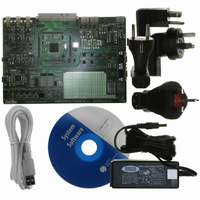
Manufacturer Part Number
EVB9S12XEP100
Description
BOARD EVAL FOR MC9S12XEP100
Manufacturer
Freescale Semiconductor
Type
MCUr
Datasheet
1.EVB9S12XEP100.pdf
(1328 pages)
Specifications of EVB9S12XEP100
Contents
Module and Misc Hardware
Processor To Be Evaluated
MC9S12XEP100
Data Bus Width
16 bit
Interface Type
RS-232
Silicon Manufacturer
Freescale
Core Architecture
S12
Core Sub-architecture
S12
Silicon Core Number
MC9S12
Silicon Family Name
S12XE
Rohs Compliant
Yes
For Use With/related Products
MC9S12XEP100
Lead Free Status / RoHS Status
Lead free / RoHS Compliant


1.9
The MPU has the option of a third bus master (CPU + XGATE + other) which is not present on this device
family but may be on other parts.
1.10
The VREGEN connection of the voltage regulator is tied internally to VDDR such that the voltage
regulator is always enabled with VDDR connected to a positive supply voltage. The device must be
configured with the internal voltage regulator enabled. Operation in conjunction with an external voltage
regulator is not supported.
The autonomous periodic interrupt clock output is mapped to PortT[5].
The API trimming register APITR is loaded on rising edge of RESET from the Flash IFR option field at
global address 0x40_00F0 bits[5:0] during the reset sequence. Currently factory programming of this IFR
range is not supported.
1.10.1
The VREG high temperature trimming register bits VREGHTTR[3:0] are loaded from the internal Flash
during the reset sequence. To use the high temperature interrupt within the specified limits (T
T
The device temperature can be monitored on ADC0 channel[17].
The internal bandgap reference voltage can also be mapped to ADC0 analog input channel[17]. The
voltage regulator VSEL bit when set, maps the bandgap and, when clear, maps the temperature sensor to
ADC0 channel[17].
Read access to reserved VREG register space returns “0”. Write accesses have no effect. This device does
not support access abort of reserved VREG register space.
1.11
The BDM alternate clock source is the oscillator clock.
1.12
On smaller derivatives the S12XEPIM module is a subset of the S12XEP100. The registers of the
unavailable ports are unimplemented.
Freescale Semiconductor
HTID
Because of an order from the United States International Trade Commission, BGA-packaged product lines and partnumbers
indicated here currently are not available from Freescale for import or sale in the United States prior to September 2010
) these bits must be loaded with 0x8. Currently factory programming is not supported.
MPU Configuration
VREG Configuration
BDM Clock Configuration
S12XEPIM Configuration
Temperature Sensor Configuration
MC9S12XE-Family Reference Manual Rev. 1.23
Chapter 1 Device Overview MC9S12XE-Family
HTIA
and
87
Related parts for EVB9S12XEP100
Image
Part Number
Description
Manufacturer
Datasheet
Request
R

Part Number:
Description:
Manufacturer:
Freescale Semiconductor, Inc
Datasheet:
Part Number:
Description:
Manufacturer:
Freescale Semiconductor, Inc
Datasheet:
Part Number:
Description:
Manufacturer:
Freescale Semiconductor, Inc
Datasheet:
Part Number:
Description:
Manufacturer:
Freescale Semiconductor, Inc
Datasheet:
Part Number:
Description:
Manufacturer:
Freescale Semiconductor, Inc
Datasheet:
Part Number:
Description:
Manufacturer:
Freescale Semiconductor, Inc
Datasheet:
Part Number:
Description:
Manufacturer:
Freescale Semiconductor, Inc
Datasheet:
Part Number:
Description:
Manufacturer:
Freescale Semiconductor, Inc
Datasheet:
Part Number:
Description:
Manufacturer:
Freescale Semiconductor, Inc
Datasheet:
Part Number:
Description:
Manufacturer:
Freescale Semiconductor, Inc
Datasheet:
Part Number:
Description:
Manufacturer:
Freescale Semiconductor, Inc
Datasheet:
Part Number:
Description:
Manufacturer:
Freescale Semiconductor, Inc
Datasheet:
Part Number:
Description:
Manufacturer:
Freescale Semiconductor, Inc
Datasheet:
Part Number:
Description:
Manufacturer:
Freescale Semiconductor, Inc
Datasheet:
Part Number:
Description:
Manufacturer:
Freescale Semiconductor, Inc
Datasheet: