EVB9S12XEP100 Freescale Semiconductor, EVB9S12XEP100 Datasheet - Page 779
EVB9S12XEP100
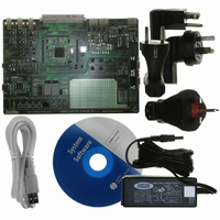
Manufacturer Part Number
EVB9S12XEP100
Description
BOARD EVAL FOR MC9S12XEP100
Manufacturer
Freescale Semiconductor
Type
MCUr
Datasheet
1.EVB9S12XEP100.pdf
(1328 pages)
Specifications of EVB9S12XEP100
Contents
Module and Misc Hardware
Processor To Be Evaluated
MC9S12XEP100
Data Bus Width
16 bit
Interface Type
RS-232
Silicon Manufacturer
Freescale
Core Architecture
S12
Core Sub-architecture
S12
Silicon Core Number
MC9S12
Silicon Family Name
S12XE
Rohs Compliant
Yes
For Use With/related Products
MC9S12XEP100
Lead Free Status / RoHS Status
Lead free / RoHS Compliant


The CPOL clock polarity control bit specifies an active high or low clock and has no significant effect on
the transmission format.
The CPHA clock phase control bit selects one of two fundamentally different transmission formats.
Clock phase and polarity should be identical for the master SPI device and the communicating slave
device. In some cases, the phase and polarity are changed between transmissions to allow a master device
to communicate with peripheral slaves having different requirements.
21.4.3.2
The first edge on the SCK line is used to clock the first data bit of the slave into the master and the first
data bit of the master into the slave. In some peripherals, the first bit of the slave’s data is available at the
slave’s data out pin as soon as the slave is selected. In this format, the first SCK edge is issued a half cycle
after SS has become low.
A half SCK cycle later, the second edge appears on the SCK line. When this second edge occurs, the value
previously latched from the serial data input pin is shifted into the LSB or MSB of the shift register,
depending on LSBFE bit.
After this second edge, the next bit of the SPI master data is transmitted out of the serial data output pin of
the master to the serial input pin on the slave. This process continues for a total of 16 edges on the SCK
line, with data being latched on odd numbered edges and shifted on even numbered edges.
Data reception is double buffered. Data is shifted serially into the SPI shift register during the transfer and
is transferred to the parallel SPI data register after the last bit is shifted in.
After 2n
Figure 21-12
CPOL = 0 and CPOL = 1. The diagram may be interpreted as a master or slave timing diagram because
the SCK, MISO, and MOSI pins are connected directly between the master and the slave. The MISO signal
is the output from the slave and the MOSI signal is the output from the master. The SS pin of the master
must be either high or reconfigured as a general-purpose output not affecting the SPI.
1. n depends on the selected transfer width, please refer to
Freescale Semiconductor
Because of an order from the United States International Trade Commission, BGA-packaged product lines and partnumbers
indicated here currently are not available from Freescale for import or sale in the United States prior to September 2010
•
•
Data that was previously in the master SPI data register should now be in the slave data register and
the data that was in the slave data register should be in the master.
The SPIF flag in the SPI status register is set, indicating that the transfer is complete.
1
(last) SCK edges:
CPHA = 0 Transfer Format
is a timing diagram of an SPI transfer where CPHA = 0. SCK waveforms are shown for
MC9S12XE-Family Reference Manual Rev. 1.23
Section 21.3.2.2, “SPI Control Register 2 (SPICR2)
Chapter 21 Serial Peripheral Interface (S12SPIV5)
779
Related parts for EVB9S12XEP100
Image
Part Number
Description
Manufacturer
Datasheet
Request
R

Part Number:
Description:
Manufacturer:
Freescale Semiconductor, Inc
Datasheet:
Part Number:
Description:
Manufacturer:
Freescale Semiconductor, Inc
Datasheet:
Part Number:
Description:
Manufacturer:
Freescale Semiconductor, Inc
Datasheet:
Part Number:
Description:
Manufacturer:
Freescale Semiconductor, Inc
Datasheet:
Part Number:
Description:
Manufacturer:
Freescale Semiconductor, Inc
Datasheet:
Part Number:
Description:
Manufacturer:
Freescale Semiconductor, Inc
Datasheet:
Part Number:
Description:
Manufacturer:
Freescale Semiconductor, Inc
Datasheet:
Part Number:
Description:
Manufacturer:
Freescale Semiconductor, Inc
Datasheet:
Part Number:
Description:
Manufacturer:
Freescale Semiconductor, Inc
Datasheet:
Part Number:
Description:
Manufacturer:
Freescale Semiconductor, Inc
Datasheet:
Part Number:
Description:
Manufacturer:
Freescale Semiconductor, Inc
Datasheet:
Part Number:
Description:
Manufacturer:
Freescale Semiconductor, Inc
Datasheet:
Part Number:
Description:
Manufacturer:
Freescale Semiconductor, Inc
Datasheet:
Part Number:
Description:
Manufacturer:
Freescale Semiconductor, Inc
Datasheet:
Part Number:
Description:
Manufacturer:
Freescale Semiconductor, Inc
Datasheet: