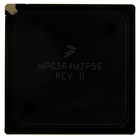
MPC564MZP56 Freescale Semiconductor, MPC564MZP56 Datasheet - Page 150

MPC564MZP56
Manufacturer Part Number
MPC564MZP56
Description
IC MCU 512K FLASH 56MHZ 388-BGA
Manufacturer
Freescale Semiconductor
Series
MPC5xxr
Specifications of MPC564MZP56
Core Processor
PowerPC
Core Size
32-Bit
Speed
56MHz
Connectivity
CAN, EBI/EMI, SCI, SPI, UART/USART
Peripherals
POR, PWM, WDT
Number Of I /o
56
Program Memory Size
512KB (512K x 8)
Program Memory Type
FLASH
Ram Size
32K x 8
Voltage - Supply (vcc/vdd)
2.5 V ~ 2.7 V
Data Converters
A/D 32x10b
Oscillator Type
External
Operating Temperature
-40°C ~ 125°C
Package / Case
388-BGA
Core
PowerPC
Processor Series
MPC5xx
Data Bus Width
32 bit
Maximum Clock Frequency
56 MHz
Data Ram Size
32 KB
On-chip Adc
Yes
Number Of Programmable I/os
56
Number Of Timers
2
Operating Supply Voltage
0 V to 5 V
Mounting Style
SMD/SMT
A/d Bit Size
10 bit
A/d Channels Available
32
Height
1.95 mm
Interface Type
CAN, JTAG, QSPI, SCI, SPI, UART
Length
27 mm
Maximum Operating Temperature
+ 125 C
Minimum Operating Temperature
- 40 C
Supply Voltage (max)
2.7 V, 5.25 V
Supply Voltage (min)
2.5 V, 4.75 V
Width
27 mm
For Use With
MPC564EVB - KIT EVAL FOR MPC561/562/563/564
Lead Free Status / RoHS Status
Contains lead / RoHS non-compliant
Eeprom Size
-
Lead Free Status / Rohs Status
No RoHS Version Available
Available stocks
Company
Part Number
Manufacturer
Quantity
Price
Company:
Part Number:
MPC564MZP56
Manufacturer:
FREESCAL
Quantity:
364
Company:
Part Number:
MPC564MZP56
Manufacturer:
Freescale Semiconductor
Quantity:
10 000
Part Number:
MPC564MZP56
Manufacturer:
FREESCALE
Quantity:
20 000
Company:
Part Number:
MPC564MZP56R2
Manufacturer:
Freescale Semiconductor
Quantity:
10 000
- Current page: 150 of 1420
- Download datasheet (11Mb)
Central Processing Unit
on consecutive clock cycles. Divide instructions are not pipelined; an integer divide instruction preceded
or followed by an integer divide or multiply instruction results in a processor-pipeline stall. However, since
IMUL–IDIV and ALU–BFU are implemented as separate execution units, an integer divide instruction
preceded or followed by an ALU–BFU instruction does not cause a delay in the pipeline.
3.4.3
The load/store unit handles all data transfer between the general-purpose register file and the internal
load/store bus (L-bus). The load/store unit is implemented as an independent execution unit so that stalls
in the memory pipeline do not stall the master instruction pipeline (unless there is a data dependency). The
unit is fully pipelined so that memory instructions of any size may be issued on back-to-back cycles.
There is a 32-bit wide data path between the load/store unit and the general-purpose register file.
Single-word accesses can be achieved with an internal on-chip data RAM, resulting in a two-clock latency.
Double-word accesses require two clocks, resulting in a three-clock latency. Since the L-bus is 32 bits
wide, double-word transfers require two bus accesses. The load/store unit performs zero-fill for byte and
half-word transfers and sign extension for half-word transfers.
Addresses are formed by adding the source-one register operand specified by the instruction (or zero) to
either a source-two register operand or to a 16-bit, immediate value embedded in the instruction.
3.4.4
The FPU contains a double-precision multiply array, the floating-point status and control register
(FPSCR), and the FPRs. The multiply-add array allows the RCPU to efficiently implement floating-point
operations such as multiply, multiply-add, and divide.
The RCPU depends on a software envelope to fully implement the IEEE floating-point specification.
Overflows, underflows, NaNs (not a number), and denormalized numbers cause floating-point assist
exceptions that invoke a software routine to deliver (with hardware assistance) the correct IEEE result.
To accelerate time-critical operations and make them more deterministic, the RCPU provides a mode of
operation that avoids invoking a software envelope and attempts to deliver results in hardware that are
adequate for most applications, if not in strict compliance with IEEE standards. In this mode, denormalized
numbers, NaNs, and IEEE invalid operations are legitimate, returning default results rather than causing
floating-point assist exceptions.
3.5
The PowerPC ISA architecture consists of three levels:
3-6
•
•
User instruction set architecture (UISA) — defines the base user-level instruction set, user-level
registers, data types, floating-point exception model, memory models for a uniprocessor
environment, and programming model for a uniprocessor environment.
Virtual environment architecture (VEA) — describes the memory model for a multiprocessor
environment, and describes other aspects of virtual environments.
Implementations that conform to the VEA also adhere to the UISA, but may not necessarily adhere
to the OEA.
Levels of the PowerPC ISA Architecture
Load/Store Unit (LSU)
Floating-Point Unit (FPU)
MPC561/MPC563 Reference Manual, Rev. 1.2
Freescale Semiconductor
Related parts for MPC564MZP56
Image
Part Number
Description
Manufacturer
Datasheet
Request
R

Part Number:
Description:
MPC5 1K0 5%
Manufacturer:
TE Connectivity
Datasheet:

Part Number:
Description:
MPC5 500R 5%
Manufacturer:
TE Connectivity
Datasheet:

Part Number:
Description:
MPC5 5K0 5%
Manufacturer:
Tyco Electronics
Datasheet:

Part Number:
Description:
MPC5 5R0 5%
Manufacturer:
Tyco Electronics
Datasheet:

Part Number:
Description:
MPC5 50K 5%
Manufacturer:
Tyco Electronics
Datasheet:

Part Number:
Description:
MPC5 1R0 5%
Manufacturer:
Tyco Electronics
Datasheet:
Part Number:
Description:
Manufacturer:
Freescale Semiconductor, Inc
Datasheet:
Part Number:
Description:
Manufacturer:
Freescale Semiconductor, Inc
Datasheet:
Part Number:
Description:
Manufacturer:
Freescale Semiconductor, Inc
Datasheet:
Part Number:
Description:
Manufacturer:
Freescale Semiconductor, Inc
Datasheet:
Part Number:
Description:
Manufacturer:
Freescale Semiconductor, Inc
Datasheet:


