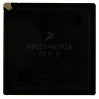
MPC564MZP56 Freescale Semiconductor, MPC564MZP56 Datasheet - Page 886

MPC564MZP56
Manufacturer Part Number
MPC564MZP56
Description
IC MCU 512K FLASH 56MHZ 388-BGA
Manufacturer
Freescale Semiconductor
Series
MPC5xxr
Specifications of MPC564MZP56
Core Processor
PowerPC
Core Size
32-Bit
Speed
56MHz
Connectivity
CAN, EBI/EMI, SCI, SPI, UART/USART
Peripherals
POR, PWM, WDT
Number Of I /o
56
Program Memory Size
512KB (512K x 8)
Program Memory Type
FLASH
Ram Size
32K x 8
Voltage - Supply (vcc/vdd)
2.5 V ~ 2.7 V
Data Converters
A/D 32x10b
Oscillator Type
External
Operating Temperature
-40°C ~ 125°C
Package / Case
388-BGA
Core
PowerPC
Processor Series
MPC5xx
Data Bus Width
32 bit
Maximum Clock Frequency
56 MHz
Data Ram Size
32 KB
On-chip Adc
Yes
Number Of Programmable I/os
56
Number Of Timers
2
Operating Supply Voltage
0 V to 5 V
Mounting Style
SMD/SMT
A/d Bit Size
10 bit
A/d Channels Available
32
Height
1.95 mm
Interface Type
CAN, JTAG, QSPI, SCI, SPI, UART
Length
27 mm
Maximum Operating Temperature
+ 125 C
Minimum Operating Temperature
- 40 C
Supply Voltage (max)
2.7 V, 5.25 V
Supply Voltage (min)
2.5 V, 4.75 V
Width
27 mm
For Use With
MPC564EVB - KIT EVAL FOR MPC561/562/563/564
Lead Free Status / RoHS Status
Contains lead / RoHS non-compliant
Eeprom Size
-
Lead Free Status / Rohs Status
No RoHS Version Available
Available stocks
Company
Part Number
Manufacturer
Quantity
Price
Company:
Part Number:
MPC564MZP56
Manufacturer:
FREESCAL
Quantity:
364
Company:
Part Number:
MPC564MZP56
Manufacturer:
Freescale Semiconductor
Quantity:
10 000
Part Number:
MPC564MZP56
Manufacturer:
FREESCALE
Quantity:
20 000
Company:
Part Number:
MPC564MZP56R2
Manufacturer:
Freescale Semiconductor
Quantity:
10 000
- Current page: 886 of 1420
- Download datasheet (11Mb)
CDR3 Flash (UC3F) EEPROM
21.3.7.2
Programming the shadow information uses the same procedure as programming the array except that SIE
must be set to a 1 prior to initiating the programming sequence. Only the lowermost addresses are used to
encode words that get programmed in the shadow row. The shadow information is physically located in
21-24
State
S2
S3
S4
S5
First Program Hardware Interlock Write:
Normal read operation still occurs. The array will
accept programming writes. Accesses to the
registers are normal register accesses. A write to
UC3FCTL cannot change EHV at this time.If the
write is to a register no data will be stored in the
program data latch and the UC3F remains in state
S2.
Expanded Program Hardware Interlock Operation:
Programming writes are accepted so that data
may be programmed. These writes may be to any
UC3F array location. The location to be
programmed is determined from the address
initially written to on the first program interlock
write. The program data latch may be updated on
any program interlock writes which occur in this
state. Accesses to the registers are normal
register accesses. A write to UC3FCTL can
change EHV. If the write is to a register no data will
be stored in the program data latch.
Program Operation:
High voltage is applied to the array or shadow
information to program the UC3F bit cells, and
program margin reads are automatically
performed by the internal program control logic.
No further programming writes will be accepted.
During programming, the array will not respond to
any access. Accesses to the registers are allowed.
A write to UC3FCTL can change EHV or HSUS
only.
Program Suspend Operation:
The program operation is suspended to either
read the array or disable the module. Once HVS
reads as a 0, the program operation is suspended.
Normal reads to the array can be performed if the
module is enabled; read accesses to the location
being programmed returns indeterminate data.
Program Shadow Information
Table 21-7. Program Interlock State Descriptions (continued)
Mode
MPC561/MPC563 Reference Manual, Rev. 1.2
State
Next
S1
S3
S1
S4
S1
S2
S5
S1
S4
T10
T1
T3
T6
T4
T5
T7
T8
T9
Write SES = 0 or a reset.
Hardware Interlock. A successful write
to any UC3F array location. This
programming write will latch the
selected word of data into the program
data latch and the address is latched
to select the location that will be
programmed. Once a bit has been
written then it remains in the program
data latch until another write
over-writes that data or a write of SES
= 0. If the write is to a register no data
will be stored in the program data latch
and the UC3F remains in state S2.
Write SES = 0 or a reset.
Write EHV = 1.
Reset.
Write EHV = 0.
Write HSUS = 1 or disable the UC3F
module.
Reset.
Write HSUS = 0 or re-enable the
UC3F module.
Transition Requirement
Freescale Semiconductor
Related parts for MPC564MZP56
Image
Part Number
Description
Manufacturer
Datasheet
Request
R

Part Number:
Description:
MPC5 1K0 5%
Manufacturer:
TE Connectivity
Datasheet:

Part Number:
Description:
MPC5 500R 5%
Manufacturer:
TE Connectivity
Datasheet:

Part Number:
Description:
MPC5 5K0 5%
Manufacturer:
Tyco Electronics
Datasheet:

Part Number:
Description:
MPC5 5R0 5%
Manufacturer:
Tyco Electronics
Datasheet:

Part Number:
Description:
MPC5 50K 5%
Manufacturer:
Tyco Electronics
Datasheet:

Part Number:
Description:
MPC5 1R0 5%
Manufacturer:
Tyco Electronics
Datasheet:
Part Number:
Description:
Manufacturer:
Freescale Semiconductor, Inc
Datasheet:
Part Number:
Description:
Manufacturer:
Freescale Semiconductor, Inc
Datasheet:
Part Number:
Description:
Manufacturer:
Freescale Semiconductor, Inc
Datasheet:
Part Number:
Description:
Manufacturer:
Freescale Semiconductor, Inc
Datasheet:
Part Number:
Description:
Manufacturer:
Freescale Semiconductor, Inc
Datasheet:


