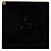
MPC564MZP56 Freescale Semiconductor, MPC564MZP56 Datasheet - Page 822

MPC564MZP56
Manufacturer Part Number
MPC564MZP56
Description
IC MCU 512K FLASH 56MHZ 388-BGA
Manufacturer
Freescale Semiconductor
Series
MPC5xxr
Specifications of MPC564MZP56
Core Processor
PowerPC
Core Size
32-Bit
Speed
56MHz
Connectivity
CAN, EBI/EMI, SCI, SPI, UART/USART
Peripherals
POR, PWM, WDT
Number Of I /o
56
Program Memory Size
512KB (512K x 8)
Program Memory Type
FLASH
Ram Size
32K x 8
Voltage - Supply (vcc/vdd)
2.5 V ~ 2.7 V
Data Converters
A/D 32x10b
Oscillator Type
External
Operating Temperature
-40°C ~ 125°C
Package / Case
388-BGA
Core
PowerPC
Processor Series
MPC5xx
Data Bus Width
32 bit
Maximum Clock Frequency
56 MHz
Data Ram Size
32 KB
On-chip Adc
Yes
Number Of Programmable I/os
56
Number Of Timers
2
Operating Supply Voltage
0 V to 5 V
Mounting Style
SMD/SMT
A/d Bit Size
10 bit
A/d Channels Available
32
Height
1.95 mm
Interface Type
CAN, JTAG, QSPI, SCI, SPI, UART
Length
27 mm
Maximum Operating Temperature
+ 125 C
Minimum Operating Temperature
- 40 C
Supply Voltage (max)
2.7 V, 5.25 V
Supply Voltage (min)
2.5 V, 4.75 V
Width
27 mm
For Use With
MPC564EVB - KIT EVAL FOR MPC561/562/563/564
Lead Free Status / RoHS Status
Contains lead / RoHS non-compliant
Eeprom Size
-
Lead Free Status / Rohs Status
No RoHS Version Available
Available stocks
Company
Part Number
Manufacturer
Quantity
Price
Company:
Part Number:
MPC564MZP56
Manufacturer:
FREESCAL
Quantity:
364
Company:
Part Number:
MPC564MZP56
Manufacturer:
Freescale Semiconductor
Quantity:
10 000
Part Number:
MPC564MZP56
Manufacturer:
FREESCALE
Quantity:
20 000
Company:
Part Number:
MPC564MZP56R2
Manufacturer:
Freescale Semiconductor
Quantity:
10 000
- Current page: 822 of 1420
- Download datasheet (11Mb)
Peripheral Pin Multiplexing (PPM) Module
TX_CONFIG_1 and TX_CONFIG_2 can only be written while PPM transmit mode is disabled
(PPMPCR[ENTX] = 0). While transmit is enabled these registers read as 0x00 and writing them will return
TEA (bus error access).
18.4.4
The two receive configuration registers control which internal modules will receive data from the PPM.
Each of the configuration registers contains eight separate 2-bit wide bit fields. Each of the 16 fields
controls a multiplexer that selects a 1-bit channel from the PPM data receive register to an internal module.
See
RX_CONFIG_1 and RX_CONFIG_2 can only be written while PPM receive mode is disabled
(PPMPCR[ENRX] = 0). While receive mode is enabled these registers read as 0x00 and writing them will
return TEA (bus error access).
18-16
SRESET
SRESET
SRESET
Table 18-6
Field
Field
Addr
Addr
Field
Addr
Receive Configuration Registers (RX_CONFIG_1 and
RX_CONFIG_2)
MSB
MSB
MSB
0
0
0
CH15
CH7
CH7
for more information on channel control and setting the channel values.
1
1
1
Figure 18-14. Transmit Configuration Register 1 (TX_CONFIG_1)
Figure 18-15. Transmit Configuration Register 2 (TX_CONFIG_2)
Figure 18-16. Receive Configuration Register 1 (RX_CONFIG_1)
2
2
2
CH14
CH6
CH6
3
3
3
MPC561/MPC563 Reference Manual, Rev. 1.2
4
4
4
CH13
CH5
CH5
5
5
5
0000_0000_0000_0000
0000_0000_0000_0000
0000_0000_0000_0000
6
6
6
CH12
CH4
CH4
0x30 5C06
0x30 5C08
0x30 5C0E
7
7
7
8
8
8
CH11
CH3
CH3
9
9
9
10
10
10
CH10
CH2
CH2
11
11
11
12
12
12
CH9
CH1
CH1
Freescale Semiconductor
13
13
13
14
14
14
CH0
CH8
CH0
LSB
LSB
LSB
15
15
15
Related parts for MPC564MZP56
Image
Part Number
Description
Manufacturer
Datasheet
Request
R

Part Number:
Description:
MPC5 1K0 5%
Manufacturer:
TE Connectivity
Datasheet:

Part Number:
Description:
MPC5 500R 5%
Manufacturer:
TE Connectivity
Datasheet:

Part Number:
Description:
MPC5 5K0 5%
Manufacturer:
Tyco Electronics
Datasheet:

Part Number:
Description:
MPC5 5R0 5%
Manufacturer:
Tyco Electronics
Datasheet:

Part Number:
Description:
MPC5 50K 5%
Manufacturer:
Tyco Electronics
Datasheet:

Part Number:
Description:
MPC5 1R0 5%
Manufacturer:
Tyco Electronics
Datasheet:
Part Number:
Description:
Manufacturer:
Freescale Semiconductor, Inc
Datasheet:
Part Number:
Description:
Manufacturer:
Freescale Semiconductor, Inc
Datasheet:
Part Number:
Description:
Manufacturer:
Freescale Semiconductor, Inc
Datasheet:
Part Number:
Description:
Manufacturer:
Freescale Semiconductor, Inc
Datasheet:
Part Number:
Description:
Manufacturer:
Freescale Semiconductor, Inc
Datasheet:


