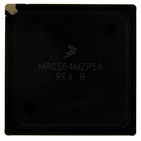
MPC564MZP56 Freescale Semiconductor, MPC564MZP56 Datasheet - Page 432

MPC564MZP56
Manufacturer Part Number
MPC564MZP56
Description
IC MCU 512K FLASH 56MHZ 388-BGA
Manufacturer
Freescale Semiconductor
Series
MPC5xxr
Specifications of MPC564MZP56
Core Processor
PowerPC
Core Size
32-Bit
Speed
56MHz
Connectivity
CAN, EBI/EMI, SCI, SPI, UART/USART
Peripherals
POR, PWM, WDT
Number Of I /o
56
Program Memory Size
512KB (512K x 8)
Program Memory Type
FLASH
Ram Size
32K x 8
Voltage - Supply (vcc/vdd)
2.5 V ~ 2.7 V
Data Converters
A/D 32x10b
Oscillator Type
External
Operating Temperature
-40°C ~ 125°C
Package / Case
388-BGA
Core
PowerPC
Processor Series
MPC5xx
Data Bus Width
32 bit
Maximum Clock Frequency
56 MHz
Data Ram Size
32 KB
On-chip Adc
Yes
Number Of Programmable I/os
56
Number Of Timers
2
Operating Supply Voltage
0 V to 5 V
Mounting Style
SMD/SMT
A/d Bit Size
10 bit
A/d Channels Available
32
Height
1.95 mm
Interface Type
CAN, JTAG, QSPI, SCI, SPI, UART
Length
27 mm
Maximum Operating Temperature
+ 125 C
Minimum Operating Temperature
- 40 C
Supply Voltage (max)
2.7 V, 5.25 V
Supply Voltage (min)
2.5 V, 4.75 V
Width
27 mm
For Use With
MPC564EVB - KIT EVAL FOR MPC561/562/563/564
Lead Free Status / RoHS Status
Contains lead / RoHS non-compliant
Eeprom Size
-
Lead Free Status / Rohs Status
No RoHS Version Available
Available stocks
Company
Part Number
Manufacturer
Quantity
Price
Company:
Part Number:
MPC564MZP56
Manufacturer:
FREESCAL
Quantity:
364
Company:
Part Number:
MPC564MZP56
Manufacturer:
Freescale Semiconductor
Quantity:
10 000
Part Number:
MPC564MZP56
Manufacturer:
FREESCALE
Quantity:
20 000
Company:
Part Number:
MPC564MZP56R2
Manufacturer:
Freescale Semiconductor
Quantity:
10 000
- Current page: 432 of 1420
- Download datasheet (11Mb)
Memory Controller
10.9.4
10-34
1,
Bits
30
31
1
It is recommended that this field hold values that are the power of 2 minus 1 (e.g., 2
HRESET
HRESET
Memory Controller Option Registers (OR0–OR3)
Field
Addr
Name
BI
V
MSB
AM
16
0
Burst inhibit
0 Memory controller drives BI negated (high). The bank supports burst accesses.
1 Memory controller drives BI asserted (low). The bank does not support burst accesses.
NOTE: Following a system reset, the BI bit is set.
Valid bit. When set, this bit indicates that the contents of the base-register and option-register
pair are valid. The CS signal does not assert until the V-bit is set.
NOTE: An access to a region that has no V-bit set may cause a bus monitor timeout. See
Table 10-9
Figure 10-24. Memory Controller Option Registers 1–3 (OR0–OR3)
17
1
Branch Register
0x2F C104 (OR0); 0x2F C10C (OR1); 0x2F C114 (OR2), 0x2F C11C (OR3)
Table 10-8. BR0–BR3 Bit Descriptions (continued)
ATM
18
2
BR0
BR1
BR2
BR3
for the reset value of this bit in BR0.
MPC561/MPC563 Reference Manual, Rev. 1.2
19
3
0000_0000
Table 10-9. BRx[V] Reset Value
CSNT
20
4
21
5
ACS
0000_0000_0000_0000
22
6
EHTR
23
7
Description
AM
1
24
8
BRx[V] Reset Value
25
ID20 & ID31
9
1111
SCY
ID3
10
26
0
0
11
27
3
- 1 = 7 [0b111]).
12
28
0
BSCY
Freescale Semiconductor
13
29
1
14
30
1
TRLX
LSB
15
31
0
Related parts for MPC564MZP56
Image
Part Number
Description
Manufacturer
Datasheet
Request
R

Part Number:
Description:
MPC5 1K0 5%
Manufacturer:
TE Connectivity
Datasheet:

Part Number:
Description:
MPC5 500R 5%
Manufacturer:
TE Connectivity
Datasheet:

Part Number:
Description:
MPC5 5K0 5%
Manufacturer:
Tyco Electronics
Datasheet:

Part Number:
Description:
MPC5 5R0 5%
Manufacturer:
Tyco Electronics
Datasheet:

Part Number:
Description:
MPC5 50K 5%
Manufacturer:
Tyco Electronics
Datasheet:

Part Number:
Description:
MPC5 1R0 5%
Manufacturer:
Tyco Electronics
Datasheet:
Part Number:
Description:
Manufacturer:
Freescale Semiconductor, Inc
Datasheet:
Part Number:
Description:
Manufacturer:
Freescale Semiconductor, Inc
Datasheet:
Part Number:
Description:
Manufacturer:
Freescale Semiconductor, Inc
Datasheet:
Part Number:
Description:
Manufacturer:
Freescale Semiconductor, Inc
Datasheet:
Part Number:
Description:
Manufacturer:
Freescale Semiconductor, Inc
Datasheet:


