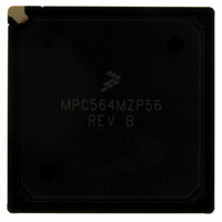
MPC564MZP56 Freescale Semiconductor, MPC564MZP56 Datasheet - Page 466

MPC564MZP56
Manufacturer Part Number
MPC564MZP56
Description
IC MCU 512K FLASH 56MHZ 388-BGA
Manufacturer
Freescale Semiconductor
Series
MPC5xxr
Specifications of MPC564MZP56
Core Processor
PowerPC
Core Size
32-Bit
Speed
56MHz
Connectivity
CAN, EBI/EMI, SCI, SPI, UART/USART
Peripherals
POR, PWM, WDT
Number Of I /o
56
Program Memory Size
512KB (512K x 8)
Program Memory Type
FLASH
Ram Size
32K x 8
Voltage - Supply (vcc/vdd)
2.5 V ~ 2.7 V
Data Converters
A/D 32x10b
Oscillator Type
External
Operating Temperature
-40°C ~ 125°C
Package / Case
388-BGA
Core
PowerPC
Processor Series
MPC5xx
Data Bus Width
32 bit
Maximum Clock Frequency
56 MHz
Data Ram Size
32 KB
On-chip Adc
Yes
Number Of Programmable I/os
56
Number Of Timers
2
Operating Supply Voltage
0 V to 5 V
Mounting Style
SMD/SMT
A/d Bit Size
10 bit
A/d Channels Available
32
Height
1.95 mm
Interface Type
CAN, JTAG, QSPI, SCI, SPI, UART
Length
27 mm
Maximum Operating Temperature
+ 125 C
Minimum Operating Temperature
- 40 C
Supply Voltage (max)
2.7 V, 5.25 V
Supply Voltage (min)
2.5 V, 4.75 V
Width
27 mm
For Use With
MPC564EVB - KIT EVAL FOR MPC561/562/563/564
Lead Free Status / RoHS Status
Contains lead / RoHS non-compliant
Eeprom Size
-
Lead Free Status / Rohs Status
No RoHS Version Available
Available stocks
Company
Part Number
Manufacturer
Quantity
Price
Company:
Part Number:
MPC564MZP56
Manufacturer:
FREESCAL
Quantity:
364
Company:
Part Number:
MPC564MZP56
Manufacturer:
Freescale Semiconductor
Quantity:
10 000
Part Number:
MPC564MZP56
Manufacturer:
FREESCALE
Quantity:
20 000
Company:
Part Number:
MPC564MZP56R2
Manufacturer:
Freescale Semiconductor
Quantity:
10 000
- Current page: 466 of 1420
- Download datasheet (11Mb)
QADC64E Legacy Mode Operation
13.2
This section gives an overview of the implementation of the two QADC64E modules on
MPC561/MPC563. It can also be used as a quick reference guide while programming the modules.
13.2.1
The analog section includes input signals, an analog multiplexer, and the sample and hold circuits. The
analog conversion is performed by the digital-to-analog converter (DAC) resistor-capacitor array and a
high-gain comparator.
The digital control section contains queue control logic to sequence the conversion process and interrupt
generation logic. Also included are the periodic/interval timer, control and status registers, the conversion
command word (CCW) table RAM, and the result table RAM.
The bus interface unit (BIU) allows the QADC64E to operate with the applications software through the
IMB3 environment.
13-2
•
•
•
•
•
•
•
•
•
•
•
•
•
•
Internal sample and hold
Directly supports up to four external multiplexers (for example the MC14051)
Up to 41 analog input channels using QADC64E external multiplexing
Programmable input sample time for various source impedances
Minimum conversion time of 7 µs (with typical QCLK frequency, 2 MHz)
Two conversion command queues with a total of 64 entries
Sub-queues possible using pause mechanism
Queue complete and pause software interrupts available on both queues
Queue pointers indicate current location for each queue
Automated queue modes initiated by
— External edge trigger
— Periodic/Interval timer, within QADC64E module
— Software command
— External gated trigger (Queue 1 only)
Single-scan or continuous-scan of queues
64 result registers in each QADC64E module
Output readable in three formats
— Right-justified unsigned
— Left-justified signed
— Left-justified unsigned
Unused analog channels on Port A can be used as digital input/output signals, unused analog
channels on Port B can be used as digital input signals.
Key Features and Quick Reference Diagrams
Features of the QADC64E Legacy Mode Operation
MPC561/MPC563 Reference Manual, Rev. 1.2
Freescale Semiconductor
Related parts for MPC564MZP56
Image
Part Number
Description
Manufacturer
Datasheet
Request
R

Part Number:
Description:
MPC5 1K0 5%
Manufacturer:
TE Connectivity
Datasheet:

Part Number:
Description:
MPC5 500R 5%
Manufacturer:
TE Connectivity
Datasheet:

Part Number:
Description:
MPC5 5K0 5%
Manufacturer:
Tyco Electronics
Datasheet:

Part Number:
Description:
MPC5 5R0 5%
Manufacturer:
Tyco Electronics
Datasheet:

Part Number:
Description:
MPC5 50K 5%
Manufacturer:
Tyco Electronics
Datasheet:

Part Number:
Description:
MPC5 1R0 5%
Manufacturer:
Tyco Electronics
Datasheet:
Part Number:
Description:
Manufacturer:
Freescale Semiconductor, Inc
Datasheet:
Part Number:
Description:
Manufacturer:
Freescale Semiconductor, Inc
Datasheet:
Part Number:
Description:
Manufacturer:
Freescale Semiconductor, Inc
Datasheet:
Part Number:
Description:
Manufacturer:
Freescale Semiconductor, Inc
Datasheet:
Part Number:
Description:
Manufacturer:
Freescale Semiconductor, Inc
Datasheet:


