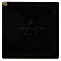
MPC564MZP56 Freescale Semiconductor, MPC564MZP56 Datasheet - Page 894

MPC564MZP56
Manufacturer Part Number
MPC564MZP56
Description
IC MCU 512K FLASH 56MHZ 388-BGA
Manufacturer
Freescale Semiconductor
Series
MPC5xxr
Specifications of MPC564MZP56
Core Processor
PowerPC
Core Size
32-Bit
Speed
56MHz
Connectivity
CAN, EBI/EMI, SCI, SPI, UART/USART
Peripherals
POR, PWM, WDT
Number Of I /o
56
Program Memory Size
512KB (512K x 8)
Program Memory Type
FLASH
Ram Size
32K x 8
Voltage - Supply (vcc/vdd)
2.5 V ~ 2.7 V
Data Converters
A/D 32x10b
Oscillator Type
External
Operating Temperature
-40°C ~ 125°C
Package / Case
388-BGA
Core
PowerPC
Processor Series
MPC5xx
Data Bus Width
32 bit
Maximum Clock Frequency
56 MHz
Data Ram Size
32 KB
On-chip Adc
Yes
Number Of Programmable I/os
56
Number Of Timers
2
Operating Supply Voltage
0 V to 5 V
Mounting Style
SMD/SMT
A/d Bit Size
10 bit
A/d Channels Available
32
Height
1.95 mm
Interface Type
CAN, JTAG, QSPI, SCI, SPI, UART
Length
27 mm
Maximum Operating Temperature
+ 125 C
Minimum Operating Temperature
- 40 C
Supply Voltage (max)
2.7 V, 5.25 V
Supply Voltage (min)
2.5 V, 4.75 V
Width
27 mm
For Use With
MPC564EVB - KIT EVAL FOR MPC561/562/563/564
Lead Free Status / RoHS Status
Contains lead / RoHS non-compliant
Eeprom Size
-
Lead Free Status / Rohs Status
No RoHS Version Available
Available stocks
Company
Part Number
Manufacturer
Quantity
Price
Company:
Part Number:
MPC564MZP56
Manufacturer:
FREESCAL
Quantity:
364
Company:
Part Number:
MPC564MZP56
Manufacturer:
Freescale Semiconductor
Quantity:
10 000
Part Number:
MPC564MZP56
Manufacturer:
FREESCALE
Quantity:
20 000
Company:
Part Number:
MPC564MZP56R2
Manufacturer:
Freescale Semiconductor
Quantity:
10 000
- Current page: 894 of 1420
- Download datasheet (11Mb)
CDR3 Flash (UC3F) EEPROM
21.3.11.2 Setting Censor
The set operation changes the state in an NVM CAM cell from a 0 to a 1. This set operation can be done
without changing the contents of the UC3F array. The required sequence to set one or both of the bits in
CENSOR[0:1] follows.
21.3.11.3 Clearing Censor
The clear operation changes the state of the CENSOR[0:1] bits from a 1 to a 0 by erasing the CAM cells.
This clear operation can be done only while erasing the entire UC3F array and shadow information. The
required sequence to clear CENSOR follows.
Clear CENSOR[0:1]
21-32
1. Write CSC = 1, PE = 0 and SES = 1 in the UC3FCTL register
2. Write a 1 to the CENSOR bit(s) to be set
3. Write EHV = 1 in the UC3FCTL register
4. Read the UC3FCTL register until HVS = 0
5. Read the UC3FCTL register. Confirm PEGOOD = 1
6. Write EHV = 0 in the UC3FCTL register
7. Write SES = 0 and CSC = 0
1. Write PROTECT[0:7] = 0x00 to enable the entire array for erase. If SBEN[M] = 1, then
2. Write BLOCK[0:7] = 0xFF, CSC = 1, PE = 1 and SES = 1 in the UC3FCTL register. If SBEN[M]
3. Do an erase interlock write.
4. Write EHV = 1 in the UC3FCTL register.
SBPROTECT[M] must also be cleared to 0.
= 1, then SBBLOCK[M] must also be set to 1.
On the UC3F module, the erase interlock write can be performed in one of two ways, depending
on the value of the UC3FCFIG bit 15, IWS.
If IWS = 0, a valid erase interlock write is a write to any valid array location. This is subject to any
censorship conditions that might apply.
If IWS = 1, a valid erase interlock write can be a write to any valid array location or a write to the
UC3FCMCR register.
When the IWS = 1, the CENSOR[0:1] bits can always be cleared in the UC3F flash EEPROM
status states #3, #4 and #5 from
The erase interlock write is only valid if all blocks of the array are selected for erase and not
protected. BLOCK[0:7] and SBBLOCK[0:1] set to 1, as well as PROTECT[0:7] and
SBPROTECT[0:1] set to 0, are required for a valid erase interlock write during the clear censor
operation.
MPC561/MPC563 Reference Manual, Rev. 1.2
Table
21-10.
Freescale Semiconductor
Related parts for MPC564MZP56
Image
Part Number
Description
Manufacturer
Datasheet
Request
R

Part Number:
Description:
MPC5 1K0 5%
Manufacturer:
TE Connectivity
Datasheet:

Part Number:
Description:
MPC5 500R 5%
Manufacturer:
TE Connectivity
Datasheet:

Part Number:
Description:
MPC5 5K0 5%
Manufacturer:
Tyco Electronics
Datasheet:

Part Number:
Description:
MPC5 5R0 5%
Manufacturer:
Tyco Electronics
Datasheet:

Part Number:
Description:
MPC5 50K 5%
Manufacturer:
Tyco Electronics
Datasheet:

Part Number:
Description:
MPC5 1R0 5%
Manufacturer:
Tyco Electronics
Datasheet:
Part Number:
Description:
Manufacturer:
Freescale Semiconductor, Inc
Datasheet:
Part Number:
Description:
Manufacturer:
Freescale Semiconductor, Inc
Datasheet:
Part Number:
Description:
Manufacturer:
Freescale Semiconductor, Inc
Datasheet:
Part Number:
Description:
Manufacturer:
Freescale Semiconductor, Inc
Datasheet:
Part Number:
Description:
Manufacturer:
Freescale Semiconductor, Inc
Datasheet:


