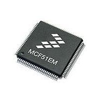
MCF51EM128CLL Freescale Semiconductor, MCF51EM128CLL Datasheet - Page 150

MCF51EM128CLL
Manufacturer Part Number
MCF51EM128CLL
Description
IC MCU 32BIT 128KB FLASH 100LQFP
Manufacturer
Freescale Semiconductor
Series
MCF51EMr
Datasheets
1.MCF51EM128CLL.pdf
(2 pages)
2.MCF51EM128CLL.pdf
(54 pages)
3.MCF51EM128CLL.pdf
(636 pages)
Specifications of MCF51EM128CLL
Core Processor
Coldfire V1
Core Size
32-Bit
Speed
50MHz
Connectivity
I²C, SCI, SPI
Peripherals
LCD, LVD, PWM, WDT
Number Of I /o
63
Program Memory Size
128KB (128K x 8)
Program Memory Type
FLASH
Ram Size
8K x 8
Voltage - Supply (vcc/vdd)
1.8 V ~ 3.6 V
Data Converters
A/D 16x12b
Oscillator Type
External
Operating Temperature
-40°C ~ 85°C
Package / Case
100-LQFP
Processor Series
MCF51EM
Core
ColdFire V1
Data Bus Width
32 bit
Data Ram Size
16 KB
Interface Type
RS-232, LIN
Maximum Clock Frequency
50 MHz
Number Of Timers
3
Operating Supply Voltage
1.8 V to 3.6 V
Maximum Operating Temperature
+ 85 C
Mounting Style
SMD/SMT
3rd Party Development Tools
JLINK-CF-BDM26, EWCF
Development Tools By Supplier
TWR-MCF51CN-KIT, TWR-SER, TWR-ELEV, TOWER
Minimum Operating Temperature
- 40 C
Lead Free Status / RoHS Status
Lead free / RoHS Compliant
Eeprom Size
-
Lead Free Status / Rohs Status
Lead free / RoHS Compliant
Available stocks
Company
Part Number
Manufacturer
Quantity
Price
Company:
Part Number:
MCF51EM128CLL
Manufacturer:
Freescale Semiconductor
Quantity:
10 000
- Current page: 150 of 636
- Download datasheet (11Mb)
Rapid GPIO (RGPIO)
5.4
The RGPIO module is a relatively-simple design with its behavior controlled by the program-visible
registers defined within its programming model.
The RGPIO module is connected to the processor’s local two-stage pipelined bus with the stages of the
ColdFire core’s operand execution pipeline (OEP) mapped directly onto the bus. This structure allows the
processor access to the RGPIO module for single-cycle pipelined reads and writes with a zero wait-state
response (as viewed in the system bus data phase stage).
5.5
The reset state of the RGPIO module disables the entire 16-bit data port. Prior to using the RGPIO port,
software typically:
5.6
This section examines the relative performance of the RGPIO output pins for two simple applications
In both applications, the relative speed of the GPIO output is presented as a function of the location of the
output bit (RGPIO versus peripheral bus GPIO).
5.6.1
In this example, several different instruction loops are executed, each generating a square-wave output
with a 50% duty cycle. For this analysis, the executed code is mapped into the processor’s RAM. This
configuration is selected to remove any jitter from the output square wave caused by the limitations
defined by the two-cycle flash memory accesses and restrictions on the initiation of a flash access. The
following instruction loops were studied:
5-10
Field
15–0
TOG
•
•
•
•
•
•
Enables the appropriate pins in RGPIO_ENB
Configures the pin direction in RGPIO_DIR
Defines the contents of the data register (RGPIO_DATA)
The processor executes a loop to toggle an output pin for a specific number of cycles, producing a
square-wave output
The processor transmits a 16-bit message using a three-pin SPI-like interface with a serial clock,
serial chip select, and serial data bit.
BCHG_LOOP — In this loop, a bit change instruction was executed using the GPIO data byte as
the operand. This instruction performs a read-modify-write operation and inverts the addressed bit.
RGPIO toggle data.
0 No effect
1 Inverts the corresponding bit in RGPIO_DATA
Functional Description
Initialization Information
Application Information
Application 1: Simple Square-Wave Generation
MCF51EM256 Series ColdFire Integrated Microcontroller Reference Manual, Rev. 8
Table 5-10. RGPIO_TOG Field Descriptions
Description
Freescale Semiconductor
Related parts for MCF51EM128CLL
Image
Part Number
Description
Manufacturer
Datasheet
Request
R

Part Number:
Description:
IC MCU 32BIT 256KB FLASH 100LQFP
Manufacturer:
Freescale Semiconductor
Datasheet:

Part Number:
Description:
BOARD DEMO HARDWARE ONLY
Manufacturer:
Freescale Semiconductor
Datasheet:

Part Number:
Description:
IC MCU 32BIT 128KB FLASH 80LQFP
Manufacturer:
Freescale Semiconductor
Datasheet:

Part Number:
Description:
IC MCU 32BIT 256KB FLASH 80LQFP
Manufacturer:
Freescale Semiconductor
Datasheet:
Part Number:
Description:
Manufacturer:
Freescale Semiconductor, Inc
Datasheet:
Part Number:
Description:
Manufacturer:
Freescale Semiconductor, Inc
Datasheet:
Part Number:
Description:
Manufacturer:
Freescale Semiconductor, Inc
Datasheet:
Part Number:
Description:
Manufacturer:
Freescale Semiconductor, Inc
Datasheet:
Part Number:
Description:
Manufacturer:
Freescale Semiconductor, Inc
Datasheet:
Part Number:
Description:
Manufacturer:
Freescale Semiconductor, Inc
Datasheet:
Part Number:
Description:
Manufacturer:
Freescale Semiconductor, Inc
Datasheet:
Part Number:
Description:
Manufacturer:
Freescale Semiconductor, Inc
Datasheet:
Part Number:
Description:
Manufacturer:
Freescale Semiconductor, Inc
Datasheet:
Part Number:
Description:
Manufacturer:
Freescale Semiconductor, Inc
Datasheet:


