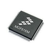
MCF51EM128CLL Freescale Semiconductor, MCF51EM128CLL Datasheet - Page 491

MCF51EM128CLL
Manufacturer Part Number
MCF51EM128CLL
Description
IC MCU 32BIT 128KB FLASH 100LQFP
Manufacturer
Freescale Semiconductor
Series
MCF51EMr
Datasheets
1.MCF51EM128CLL.pdf
(2 pages)
2.MCF51EM128CLL.pdf
(54 pages)
3.MCF51EM128CLL.pdf
(636 pages)
Specifications of MCF51EM128CLL
Core Processor
Coldfire V1
Core Size
32-Bit
Speed
50MHz
Connectivity
I²C, SCI, SPI
Peripherals
LCD, LVD, PWM, WDT
Number Of I /o
63
Program Memory Size
128KB (128K x 8)
Program Memory Type
FLASH
Ram Size
8K x 8
Voltage - Supply (vcc/vdd)
1.8 V ~ 3.6 V
Data Converters
A/D 16x12b
Oscillator Type
External
Operating Temperature
-40°C ~ 85°C
Package / Case
100-LQFP
Processor Series
MCF51EM
Core
ColdFire V1
Data Bus Width
32 bit
Data Ram Size
16 KB
Interface Type
RS-232, LIN
Maximum Clock Frequency
50 MHz
Number Of Timers
3
Operating Supply Voltage
1.8 V to 3.6 V
Maximum Operating Temperature
+ 85 C
Mounting Style
SMD/SMT
3rd Party Development Tools
JLINK-CF-BDM26, EWCF
Development Tools By Supplier
TWR-MCF51CN-KIT, TWR-SER, TWR-ELEV, TOWER
Minimum Operating Temperature
- 40 C
Lead Free Status / RoHS Status
Lead free / RoHS Compliant
Eeprom Size
-
Lead Free Status / Rohs Status
Lead free / RoHS Compliant
Available stocks
Company
Part Number
Manufacturer
Quantity
Price
Company:
Part Number:
MCF51EM128CLL
Manufacturer:
Freescale Semiconductor
Quantity:
10 000
- Current page: 491 of 636
- Download datasheet (11Mb)
The offset calibration value is automatically stored in the ADC Offset Correction Registers (ADCOFSH
and ADCOFSL) and the plus-side and minus-side calibration values are automatically stored in the ADC
Plus-Side and Minus-Side Calibration registers (CLPD, CLPS, CLP4, CLP3, CLP2, CLP1, CLP0 and
CLMD, CLMS, CLP4, CLM3, CLM2, CLM1, CLM0). The user must configure the ADC correctly prior
to calibration, and must generate the plus-side and minus-side gain calibration results and store them in the
ADC GAIN registers (ADCPGH and ADCPGL) after the calibration function completes.
Prior to calibration, the user must configure the ADC's clock frequency to be between 2 MHz and 4 MHz,
set to high speed mode (ADLPC = 0, ADHSC = 1), and set to maximum averaging (AVGE = 1,
AVGS = 11). It is recommended that calibration be run at V
conversion mode continuous function, compare function, resolution mode, and differential/single-ended
mode are all ignored during the calibration function.
To initiate calibration, the user sets the CAL bit and the calibration will automatically begin if the ADTRG
bit = 0. If ADTRG = 1, the CAL bit will not get set and the calibration fail flag (CALF) will be set. While
calibration is active, no ADC register can be written and no stop mode may be entered or the calibration
routine will be aborted causing the CAL bit to clear and the CALF bit to set. At the end of a calibration
sequence the COCO bit of the ADSC1A register will be set. The AIEN1 bit can be used to allow an
interrupt to occur at the end of a calibration sequence. If at the end of calibration routine the CALF bit is
not set, the automatic calibration routine completed successfully.
To complete calibration, the user must generate the gain calibration values using the following procedure:
When complete the user may reconfigure and use the ADC as desired. A second calibration may also be
performed if desired by clearing and again setting the CAL bit.
Overall the calibration routine may take as many as 14000 ADCK cycles and 100 bus cycles, depending
on the results and the clock source chosen. For an 8 MHz clock source this is about 1.7 msec. To reduce
this latency, the calibration values (offset, plus- and minus-side gain, and plus- and minus-side calibration
values) may be stored in flash after an initial calibration and recovered prior to the first ADC conversion.
This should reduce the calibration latency to 20 register store operations on all subsequent power, reset, or
stop2 mode recoveries.
21.5.8
The ADC Offset Correction Register (ADCOFSH:ADCOFSL) contains the user selected or calibration
generated offset error correction value. This register is a 2’s complement, left justified, 16b value formed
Freescale Semiconductor
•
•
•
•
•
•
•
Initialize (clear) a 16b variable in RAM.
Add the following plus-side calibration results CLP0, CLP1, CLP2, CLP3, CLP4, and CLPS to the
variable.
Divide the variable by two.
Set the MSB of the variable.
The previous two steps can be achieved by setting the carry bit, rotating-right through the carry bit
on the high byte and again on the low byte.
Store the value in the plus-side gain calibration registers ADCPGH and ADCPGL.
Repeat procedure for the minus-side gain calibration value.
User Defined Offset Function
MCF51EM256 Series ColdFire Integrated Microcontroller Reference Manual, Rev. 8
DDA
= V
REFH
Analog-to-Digital Converter (S08ADC16)
≥
3V. The input channel,
21-35
Related parts for MCF51EM128CLL
Image
Part Number
Description
Manufacturer
Datasheet
Request
R

Part Number:
Description:
IC MCU 32BIT 256KB FLASH 100LQFP
Manufacturer:
Freescale Semiconductor
Datasheet:

Part Number:
Description:
BOARD DEMO HARDWARE ONLY
Manufacturer:
Freescale Semiconductor
Datasheet:

Part Number:
Description:
IC MCU 32BIT 128KB FLASH 80LQFP
Manufacturer:
Freescale Semiconductor
Datasheet:

Part Number:
Description:
IC MCU 32BIT 256KB FLASH 80LQFP
Manufacturer:
Freescale Semiconductor
Datasheet:
Part Number:
Description:
Manufacturer:
Freescale Semiconductor, Inc
Datasheet:
Part Number:
Description:
Manufacturer:
Freescale Semiconductor, Inc
Datasheet:
Part Number:
Description:
Manufacturer:
Freescale Semiconductor, Inc
Datasheet:
Part Number:
Description:
Manufacturer:
Freescale Semiconductor, Inc
Datasheet:
Part Number:
Description:
Manufacturer:
Freescale Semiconductor, Inc
Datasheet:
Part Number:
Description:
Manufacturer:
Freescale Semiconductor, Inc
Datasheet:
Part Number:
Description:
Manufacturer:
Freescale Semiconductor, Inc
Datasheet:
Part Number:
Description:
Manufacturer:
Freescale Semiconductor, Inc
Datasheet:
Part Number:
Description:
Manufacturer:
Freescale Semiconductor, Inc
Datasheet:
Part Number:
Description:
Manufacturer:
Freescale Semiconductor, Inc
Datasheet:


