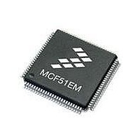
MCF51EM128CLL Freescale Semiconductor, MCF51EM128CLL Datasheet - Page 576

MCF51EM128CLL
Manufacturer Part Number
MCF51EM128CLL
Description
IC MCU 32BIT 128KB FLASH 100LQFP
Manufacturer
Freescale Semiconductor
Series
MCF51EMr
Datasheets
1.MCF51EM128CLL.pdf
(2 pages)
2.MCF51EM128CLL.pdf
(54 pages)
3.MCF51EM128CLL.pdf
(636 pages)
Specifications of MCF51EM128CLL
Core Processor
Coldfire V1
Core Size
32-Bit
Speed
50MHz
Connectivity
I²C, SCI, SPI
Peripherals
LCD, LVD, PWM, WDT
Number Of I /o
63
Program Memory Size
128KB (128K x 8)
Program Memory Type
FLASH
Ram Size
8K x 8
Voltage - Supply (vcc/vdd)
1.8 V ~ 3.6 V
Data Converters
A/D 16x12b
Oscillator Type
External
Operating Temperature
-40°C ~ 85°C
Package / Case
100-LQFP
Processor Series
MCF51EM
Core
ColdFire V1
Data Bus Width
32 bit
Data Ram Size
16 KB
Interface Type
RS-232, LIN
Maximum Clock Frequency
50 MHz
Number Of Timers
3
Operating Supply Voltage
1.8 V to 3.6 V
Maximum Operating Temperature
+ 85 C
Mounting Style
SMD/SMT
3rd Party Development Tools
JLINK-CF-BDM26, EWCF
Development Tools By Supplier
TWR-MCF51CN-KIT, TWR-SER, TWR-ELEV, TOWER
Minimum Operating Temperature
- 40 C
Lead Free Status / RoHS Status
Lead free / RoHS Compliant
Eeprom Size
-
Lead Free Status / Rohs Status
Lead free / RoHS Compliant
Available stocks
Company
Part Number
Manufacturer
Quantity
Price
Company:
Part Number:
MCF51EM128CLL
Manufacturer:
Freescale Semiconductor
Quantity:
10 000
- Current page: 576 of 636
- Download datasheet (11Mb)
Version 1 ColdFire Debug (CF1_DEBUG)
26-12
ESEQC (W)
ERASE (W)
CSTAT (R)
SEC (R)
ENBDM
CLKSW
29–27
Field
23–3
26
25
24
During reads, indicates the BDM command status.
000 Command done, no errors
001 Command done, data invalid
01x Command done, illegal
1xx Command busy, overrun
If an overrun is detected (CSTAT = 1xx), the following sequence is suggested to clear the source of the error:
1. Issue a SYNC command to reset the BDC channel.
2. The host issues a BDM NOP command.
3. The host checks the channel status using a READ_XCSR_BYTE command.
4. If XCSR[CSTAT] = 000
During writes, the ESEQC field is used for the erase sequence control during flash programming. ERASE must
also be set for this bit to have an effect.
000 User mass erase
Else Reserved
Note: See the Memory chapter for a detailed description of the algorithm for clearing security.
Select source for serial BDC communication clock.
0 Alternate, asynchronous BDC clock, typically 10 MHz
1 Synchronous bus clock (CPU clock divided by 2)
The initial state of the XCSR[CLKSW] bit is loaded by the hardware in response to certain reset events and the
state of the BKGD pin as described in
The read value of this bit typically defines the status of the flash security field.
0 Flash security is disabled
1 Flash security is enabled
In addition, the SEC bit is context-sensitive during reads. After a mass-erase sequence has been initiated by
BDM, it acts as a flash busy flag. When the erase operation is complete and the bit is cleared, it returns to reflect
the status of the chip security.
0 Flash is not busy performing a BDM mass-erase sequence
1 Flash is busy performing a BDM mass-erase sequence
During writes, this bit qualifies XCSR[ESEQC] for the write modes shown in the ESEQC field description.
0 Do not perform a mass-erase of the flash.
1 Perform a mass-erase of the flash, using the sequence specified in the XCSR[ESEQC] field.
Enable BDM.
0 BDM mode is disabled
1 Active background mode is enabled (assuming the flash is not secure)
Reserved for future use by the debug module, must be cleared.
MCF51EM256 Series ColdFire Integrated Microcontroller Reference Manual, Rev. 8
then status is okay; proceed
else
Halt the CPU with a BDM BACKGROUND command
Repeat steps 1,2,3
If XCSR[CSTAT] ≠ 000, then reset device
Table 26-7. XCSR Field Descriptions (continued)
Figure
26-2.
Description
Freescale Semiconductor
Related parts for MCF51EM128CLL
Image
Part Number
Description
Manufacturer
Datasheet
Request
R

Part Number:
Description:
IC MCU 32BIT 256KB FLASH 100LQFP
Manufacturer:
Freescale Semiconductor
Datasheet:

Part Number:
Description:
BOARD DEMO HARDWARE ONLY
Manufacturer:
Freescale Semiconductor
Datasheet:

Part Number:
Description:
IC MCU 32BIT 128KB FLASH 80LQFP
Manufacturer:
Freescale Semiconductor
Datasheet:

Part Number:
Description:
IC MCU 32BIT 256KB FLASH 80LQFP
Manufacturer:
Freescale Semiconductor
Datasheet:
Part Number:
Description:
Manufacturer:
Freescale Semiconductor, Inc
Datasheet:
Part Number:
Description:
Manufacturer:
Freescale Semiconductor, Inc
Datasheet:
Part Number:
Description:
Manufacturer:
Freescale Semiconductor, Inc
Datasheet:
Part Number:
Description:
Manufacturer:
Freescale Semiconductor, Inc
Datasheet:
Part Number:
Description:
Manufacturer:
Freescale Semiconductor, Inc
Datasheet:
Part Number:
Description:
Manufacturer:
Freescale Semiconductor, Inc
Datasheet:
Part Number:
Description:
Manufacturer:
Freescale Semiconductor, Inc
Datasheet:
Part Number:
Description:
Manufacturer:
Freescale Semiconductor, Inc
Datasheet:
Part Number:
Description:
Manufacturer:
Freescale Semiconductor, Inc
Datasheet:
Part Number:
Description:
Manufacturer:
Freescale Semiconductor, Inc
Datasheet:


