HD6417144F50V Renesas Electronics America, HD6417144F50V Datasheet - Page 45
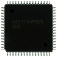
HD6417144F50V
Manufacturer Part Number
HD6417144F50V
Description
IC SUPERH MCU ROMLESS 112QFP
Manufacturer
Renesas Electronics America
Series
SuperH® SH7144r
Datasheet
1.HD64F7144F50V.pdf
(932 pages)
Specifications of HD6417144F50V
Core Processor
SH-2
Core Size
32-Bit
Speed
50MHz
Connectivity
EBI/EMI, I²C, SCI
Peripherals
DMA, POR, PWM, WDT
Number Of I /o
74
Program Memory Type
ROMless
Ram Size
8K x 8
Voltage - Supply (vcc/vdd)
3 V ~ 3.6 V
Data Converters
A/D 8x10b
Oscillator Type
Internal
Operating Temperature
-20°C ~ 75°C
Package / Case
112-QFP
For Use With
HS0005KCU11H - EMULATOR E10A-USB H8S(X),SH2(A)EDK7145 - DEV EVALUATION KIT SH7145
Lead Free Status / RoHS Status
Lead free / RoHS Compliant
Eeprom Size
-
Program Memory Size
-
Available stocks
Company
Part Number
Manufacturer
Quantity
Price
Company:

Part Number:
HD6417144F50V
Manufacturer:
Renesas Electronics America
Quantity:
10 000


Section 17 Pin Function Controller (PFC)
Table 17.1
Table 17.2
Table 17.3
Table 17.4
Table 17.5
Table 17.6
Table 17.7
Table 17.8
Table 17.9
Table 17.10
Table 17.11
Table 17.12
Table 17.13
Table 17.13
Table 17.14
Table 17.14
Table 17.15
Section 18 I/O Ports
Table 18.1
Table 18.2
Table 18.3
Table 18.4
Table 18.5
Table 18.6
Section 19 Flash Memory (F-ZTAT Version)
Table 19.1
Table 19.2
Table 19.3
Table 19.4
Table 19.5
Section 22 User Debugging Interface (H-UDI)
Table 22.1
Table 22.2
Section 23 Advanced User Debugger (AUD)
Table 23.1
Table 23.2
SH7144 Multiplexed Pins (Port A) .......................................................................569
SH7144 Multiplexed Pins (Port B) .......................................................................570
SH7144 Multiplexed Pins (Port C) .......................................................................570
SH7144 Multiplexed Pins (Port D) .......................................................................571
SH7144 Multiplexed Pins (Port E) .......................................................................572
SH7144 Multiplexed Pins (Port F)........................................................................572
SH7145 Multiplexed Pins (Port A) .......................................................................573
SH7145 Multiplexed Pins (Port B) .......................................................................574
SH7145 Multiplexed Pins (Port C) .......................................................................574
SH7145 Multiplexed Pins (Port D) .......................................................................575
SH7145 Multiplexed Pins (Port E) .......................................................................576
SH7145 Multiplexed Pins (Port F)........................................................................576
SH7144 Pin Functions in Each Mode (1) .............................................................577
SH7144 Pin Functions in Each Mode (2) .............................................................581
SH7145 Pin Functions in Each Mode (1) .............................................................585
SH7145 Pin Functions in Each Mode (2) .............................................................590
Transmit Forms of Input Functions Allocated to Multiple Pins ...........................631
Port A Data Register (PADR) Read/Write Operations .........................................638
Port B Data Register (PBDR) Read/Write Operations..........................................641
Port C Data Register (PCDR) Read/Write Operations..........................................644
Port D Data Register (PDDR) Read/Write Operations .........................................649
Port E Data Register L (PEDRL) Read/Write Operations ....................................653
Port F Data Register (PFDR) Read/Write Operations...........................................655
Differences between Boot Mode and User Program Mode...................................660
Pin Configuration..................................................................................................664
Setting On-Board Programming Modes................................................................670
Boot Mode Operation ...........................................................................................672
Peripheral Clock (Pφ) Frequencies for which Automatic Adjustment of
LSI Bit Rate Is Possible ........................................................................................672
H-UDI Pins ...........................................................................................................695
Serial Transfer Characteristics of H-UDI Registers..............................................696
AUD Pin Configuration ........................................................................................707
Ready Flag Format................................................................................................713
Rev.4.00 Mar. 27, 2008, Page xliii of xliv
REJ09B0108-0400
Related parts for HD6417144F50V
Image
Part Number
Description
Manufacturer
Datasheet
Request
R

Part Number:
Description:
KIT STARTER FOR M16C/29
Manufacturer:
Renesas Electronics America
Datasheet:

Part Number:
Description:
KIT STARTER FOR R8C/2D
Manufacturer:
Renesas Electronics America
Datasheet:

Part Number:
Description:
R0K33062P STARTER KIT
Manufacturer:
Renesas Electronics America
Datasheet:

Part Number:
Description:
KIT STARTER FOR R8C/23 E8A
Manufacturer:
Renesas Electronics America
Datasheet:

Part Number:
Description:
KIT STARTER FOR R8C/25
Manufacturer:
Renesas Electronics America
Datasheet:

Part Number:
Description:
KIT STARTER H8S2456 SHARPE DSPLY
Manufacturer:
Renesas Electronics America
Datasheet:

Part Number:
Description:
KIT STARTER FOR R8C38C
Manufacturer:
Renesas Electronics America
Datasheet:

Part Number:
Description:
KIT STARTER FOR R8C35C
Manufacturer:
Renesas Electronics America
Datasheet:

Part Number:
Description:
KIT STARTER FOR R8CL3AC+LCD APPS
Manufacturer:
Renesas Electronics America
Datasheet:
Part Number:
Description:
KIT STARTER FOR RX610
Manufacturer:
Renesas Electronics America
Datasheet:

Part Number:
Description:
KIT STARTER FOR R32C/118
Manufacturer:
Renesas Electronics America
Datasheet:

Part Number:
Description:
KIT DEV RSK-R8C/26-29
Manufacturer:
Renesas Electronics America
Datasheet:

Part Number:
Description:
KIT STARTER FOR SH7124
Manufacturer:
Renesas Electronics America
Datasheet:

Part Number:
Description:
KIT STARTER FOR H8SX/1622
Manufacturer:
Renesas Electronics America
Datasheet:

Part Number:
Description:
KIT DEV FOR SH7203
Manufacturer:
Renesas Electronics America
Datasheet: