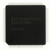
HD64F2145BTE20 Renesas Electronics America, HD64F2145BTE20 Datasheet - Page 115

HD64F2145BTE20
Manufacturer Part Number
HD64F2145BTE20
Description
IC H8S MCU FLASH 256K 100-QFP
Manufacturer
Renesas Electronics America
Series
H8® H8S/2100r
Specifications of HD64F2145BTE20
Core Processor
H8S/2000
Core Size
16-Bit
Speed
20MHz
Connectivity
I²C, IrDA, SCI, X-Bus
Peripherals
PWM, WDT
Number Of I /o
74
Program Memory Size
256KB (256K x 8)
Program Memory Type
FLASH
Ram Size
8K x 8
Voltage - Supply (vcc/vdd)
4.5 V ~ 5.5 V
Data Converters
A/D 8x10b; D/A 2x8b
Oscillator Type
Internal
Operating Temperature
-20°C ~ 75°C
Package / Case
100-TQFP, 100-VQFP
Lead Free Status / RoHS Status
Contains lead / RoHS non-compliant
Eeprom Size
-
- Current page: 115 of 847
- Download datasheet (5Mb)
2.9
2.9.1
When using the TAS instruction, use registers ER0, ER1, ER4 and ER5.
The TAS instruction is not generated by the Renesas Technology H8S and H8/300 series C/C++
compilers. When the TAS instruction is used as a user-defined intrinsic function, use registers
ER0, ER1, ER4 and ER5.
2.9.2
ER7 is not used as the register that can be saved (STM)/restored (LDM) when using STM/LDM
instruction, because ER7 is the stack pointer. Two, three, or four registers can be saved/restored by
one STM/LDM instruction. The following ranges can be specified in the register list.
Two registers: ER0–ER1, ER2–ER3, or ER4–ER5
Three registers: ER0–ER2 or ER4–ER6
Four registers: ER0–ER3
The STM/LDM instruction including ER7 is not generated by the Renesas Technology H8S and
H8/300 series C/C++ compilers.
2.9.3
The BSET, BCLR, BNOT, BST, and BIST instructions read data from the specified address in
byte units, manipulate the data of the target bit, and write data to the same address again in byte
units. Special care is required when using these instructions in cases where a register containing a
write-only bit is used or a bit is directly manipulated for a port, because this may rewrite data of a
bit other than the bit to be manipulated.
Example: The BCLR instruction is executed for DDR in port 4.
P47 and P46 are input pins, with a low-level signal input at P47 and a high-level signal input at
P46. P45 to P40 are output pins and output low-level signals. The following shows an example in
which P40 is set to be an input pin with the BCLR instruction.
Usage Notes
Note on TAS Instruction Usage
Note on STM/LDM Instruction Usage
Note on Bit Manipulation Instructions
Rev. 3.00 Mar 21, 2006 page 59 of 788
REJ09B0300-0300
Section 2 CPU
Related parts for HD64F2145BTE20
Image
Part Number
Description
Manufacturer
Datasheet
Request
R

Part Number:
Description:
KIT STARTER FOR M16C/29
Manufacturer:
Renesas Electronics America
Datasheet:

Part Number:
Description:
KIT STARTER FOR R8C/2D
Manufacturer:
Renesas Electronics America
Datasheet:

Part Number:
Description:
R0K33062P STARTER KIT
Manufacturer:
Renesas Electronics America
Datasheet:

Part Number:
Description:
KIT STARTER FOR R8C/23 E8A
Manufacturer:
Renesas Electronics America
Datasheet:

Part Number:
Description:
KIT STARTER FOR R8C/25
Manufacturer:
Renesas Electronics America
Datasheet:

Part Number:
Description:
KIT STARTER H8S2456 SHARPE DSPLY
Manufacturer:
Renesas Electronics America
Datasheet:

Part Number:
Description:
KIT STARTER FOR R8C38C
Manufacturer:
Renesas Electronics America
Datasheet:

Part Number:
Description:
KIT STARTER FOR R8C35C
Manufacturer:
Renesas Electronics America
Datasheet:

Part Number:
Description:
KIT STARTER FOR R8CL3AC+LCD APPS
Manufacturer:
Renesas Electronics America
Datasheet:

Part Number:
Description:
KIT STARTER FOR RX610
Manufacturer:
Renesas Electronics America
Datasheet:

Part Number:
Description:
KIT STARTER FOR R32C/118
Manufacturer:
Renesas Electronics America
Datasheet:

Part Number:
Description:
KIT DEV RSK-R8C/26-29
Manufacturer:
Renesas Electronics America
Datasheet:

Part Number:
Description:
KIT STARTER FOR SH7124
Manufacturer:
Renesas Electronics America
Datasheet:

Part Number:
Description:
KIT STARTER FOR H8SX/1622
Manufacturer:
Renesas Electronics America
Datasheet:

Part Number:
Description:
KIT DEV FOR SH7203
Manufacturer:
Renesas Electronics America
Datasheet:


