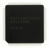
HD64F2145BTE20 Renesas Electronics America, HD64F2145BTE20 Datasheet - Page 618

HD64F2145BTE20
Manufacturer Part Number
HD64F2145BTE20
Description
IC H8S MCU FLASH 256K 100-QFP
Manufacturer
Renesas Electronics America
Series
H8® H8S/2100r
Specifications of HD64F2145BTE20
Core Processor
H8S/2000
Core Size
16-Bit
Speed
20MHz
Connectivity
I²C, IrDA, SCI, X-Bus
Peripherals
PWM, WDT
Number Of I /o
74
Program Memory Size
256KB (256K x 8)
Program Memory Type
FLASH
Ram Size
8K x 8
Voltage - Supply (vcc/vdd)
4.5 V ~ 5.5 V
Data Converters
A/D 8x10b; D/A 2x8b
Oscillator Type
Internal
Operating Temperature
-20°C ~ 75°C
Package / Case
100-TQFP, 100-VQFP
Lead Free Status / RoHS Status
Contains lead / RoHS non-compliant
Eeprom Size
-
- Current page: 618 of 847
- Download datasheet (5Mb)
Section 19 Host Interface LPC Interface (LPC)
19.4
19.4.1
The host interface is activated by setting one of bits LPC3E to LPC1E in HICR0 to 1 in single-
chip mode. When the host interface is activated, the related I/O ports (ports 37 to 30, ports 83 and
82) function as dedicated host interface input/output pins. In addition, setting the FGA20E, PMEE,
LSMIE, and LSCIE bits to 1 adds the related I/O ports (ports 81 and 80, ports B0 and B1) to the
host interface’s input/output pins.
Use the following procedure to activate the host interface after a reset release.
1. Read the signal line status and confirm that the LPC module can be connected. Also check that
2. When using channel 3, set LADR3 to determine the channel 3 I/O address and whether
3. Set the enable bit (LPC3E to LPC1E) for the channel to be used.
4. Set the enable bits (GA20E, PMEE, LSMIE, and LSCIE) for the additional functions to be
5. Set the selection bits for other functions (SDWNE, IEDIR).
6. As a precaution, clear the interrupt flags (LRST, SDWN, ABRT, OBF). Read IDR or TWR15
7. Set interrupt enable bits (IBFIE3 to IBFIE1, ERRIE) as necessary.
19.4.2
There are ten kinds of LPC transfer cycle: memory read, memory write, I/O read, I/O write, DMA
read, DMA write, bus master memory read, bus master memory write, bus master I/O read, and
bus master I/O write. Of these, the chip's LPC supports only I/O read and I/O write cycles.
An LPC transfer cycle is started when the LFRAME signal goes low in the bus idle state. If the
LFRAME signal goes low when the bus is not idle, this means that a forced termination (abort) of
the LPC transfer cycle has been requested.
In an I/O read cycle or I/O write cycle, transfer is carried out using LAD3 to LAD0 in the
following order, in synchronization with LCLK. The host can be made to wait by sending back a
value other than B 0000 in the slave’s synchronization return cycle, but with the chip’s LPC a
value of B 0000 is always returned.
Rev. 3.00 Mar 21, 2006 page 562 of 788
REJ09B0300-0300
the LPC module is initialized internally.
bidirectional data registers are to be used.
used.
to clear IBF.
Operation
Host Interface Activation
LPC I/O Cycles
Related parts for HD64F2145BTE20
Image
Part Number
Description
Manufacturer
Datasheet
Request
R

Part Number:
Description:
KIT STARTER FOR M16C/29
Manufacturer:
Renesas Electronics America
Datasheet:

Part Number:
Description:
KIT STARTER FOR R8C/2D
Manufacturer:
Renesas Electronics America
Datasheet:

Part Number:
Description:
R0K33062P STARTER KIT
Manufacturer:
Renesas Electronics America
Datasheet:

Part Number:
Description:
KIT STARTER FOR R8C/23 E8A
Manufacturer:
Renesas Electronics America
Datasheet:

Part Number:
Description:
KIT STARTER FOR R8C/25
Manufacturer:
Renesas Electronics America
Datasheet:

Part Number:
Description:
KIT STARTER H8S2456 SHARPE DSPLY
Manufacturer:
Renesas Electronics America
Datasheet:

Part Number:
Description:
KIT STARTER FOR R8C38C
Manufacturer:
Renesas Electronics America
Datasheet:

Part Number:
Description:
KIT STARTER FOR R8C35C
Manufacturer:
Renesas Electronics America
Datasheet:

Part Number:
Description:
KIT STARTER FOR R8CL3AC+LCD APPS
Manufacturer:
Renesas Electronics America
Datasheet:

Part Number:
Description:
KIT STARTER FOR RX610
Manufacturer:
Renesas Electronics America
Datasheet:

Part Number:
Description:
KIT STARTER FOR R32C/118
Manufacturer:
Renesas Electronics America
Datasheet:

Part Number:
Description:
KIT DEV RSK-R8C/26-29
Manufacturer:
Renesas Electronics America
Datasheet:

Part Number:
Description:
KIT STARTER FOR SH7124
Manufacturer:
Renesas Electronics America
Datasheet:

Part Number:
Description:
KIT STARTER FOR H8SX/1622
Manufacturer:
Renesas Electronics America
Datasheet:

Part Number:
Description:
KIT DEV FOR SH7203
Manufacturer:
Renesas Electronics America
Datasheet:


