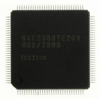
HD64F2145BTE20 Renesas Electronics America, HD64F2145BTE20 Datasheet - Page 186

HD64F2145BTE20
Manufacturer Part Number
HD64F2145BTE20
Description
IC H8S MCU FLASH 256K 100-QFP
Manufacturer
Renesas Electronics America
Series
H8® H8S/2100r
Specifications of HD64F2145BTE20
Core Processor
H8S/2000
Core Size
16-Bit
Speed
20MHz
Connectivity
I²C, IrDA, SCI, X-Bus
Peripherals
PWM, WDT
Number Of I /o
74
Program Memory Size
256KB (256K x 8)
Program Memory Type
FLASH
Ram Size
8K x 8
Voltage - Supply (vcc/vdd)
4.5 V ~ 5.5 V
Data Converters
A/D 8x10b; D/A 2x8b
Oscillator Type
Internal
Operating Temperature
-20°C ~ 75°C
Package / Case
100-TQFP, 100-VQFP
Lead Free Status / RoHS Status
Contains lead / RoHS non-compliant
Eeprom Size
-
- Current page: 186 of 847
- Download datasheet (5Mb)
Section 6 Bus Controller (BSC)
6.5.2
Table 6.4 shows the data buses used and valid strobes for each access space.
In a read, the RD signal is valid for both the upper and lower halves of the data bus. In a write, the
HWR signal is valid for the upper half of the data bus, and the LWR signal for the lower half.
Table 6.4
Area
8-bit access
space
16-bit access
space
Note: Undefined: Undefined data is output.
Rev. 3.00 Mar 21, 2006 page 130 of 788
REJ09B0300-0300
Invalid: Input state with the input value ignored.
Ports or others: Used as ports or I/O pins for on-chip peripheral modules, and are not used
as the data bus.
Figure 6.4 Access Sizes and Data Alignment Control (16-bit Access Space)
Valid Strobes
Data Buses Used and Valid Strobes
Access
Size
Byte
Byte
Word
Byte size
Byte size
Word size
Longword
size
Read/
Write
Read
Write
Read
Write
Read
Write
• Even address
• Odd address
1st bus cycle
2nd bus cycle
Address
—
—
Even
Odd
Even
Odd
—
—
Valid
Strobe
RD
HWR
RD
HWR
LWR
RD
HWR, LWR
D15
Upper data bus
Upper Data Bus
(D15 to D8)
Valid
Valid
Invalid
Valid
Undefined
Valid
Valid
D8 D7
Lower data bus
D0
Lower Data
Bus (D7 to D0)
Ports or others
Ports or others
Invalid
Valid
Undefined
Valid
Valid
Valid
Related parts for HD64F2145BTE20
Image
Part Number
Description
Manufacturer
Datasheet
Request
R

Part Number:
Description:
KIT STARTER FOR M16C/29
Manufacturer:
Renesas Electronics America
Datasheet:

Part Number:
Description:
KIT STARTER FOR R8C/2D
Manufacturer:
Renesas Electronics America
Datasheet:

Part Number:
Description:
R0K33062P STARTER KIT
Manufacturer:
Renesas Electronics America
Datasheet:

Part Number:
Description:
KIT STARTER FOR R8C/23 E8A
Manufacturer:
Renesas Electronics America
Datasheet:

Part Number:
Description:
KIT STARTER FOR R8C/25
Manufacturer:
Renesas Electronics America
Datasheet:

Part Number:
Description:
KIT STARTER H8S2456 SHARPE DSPLY
Manufacturer:
Renesas Electronics America
Datasheet:

Part Number:
Description:
KIT STARTER FOR R8C38C
Manufacturer:
Renesas Electronics America
Datasheet:

Part Number:
Description:
KIT STARTER FOR R8C35C
Manufacturer:
Renesas Electronics America
Datasheet:

Part Number:
Description:
KIT STARTER FOR R8CL3AC+LCD APPS
Manufacturer:
Renesas Electronics America
Datasheet:

Part Number:
Description:
KIT STARTER FOR RX610
Manufacturer:
Renesas Electronics America
Datasheet:

Part Number:
Description:
KIT STARTER FOR R32C/118
Manufacturer:
Renesas Electronics America
Datasheet:

Part Number:
Description:
KIT DEV RSK-R8C/26-29
Manufacturer:
Renesas Electronics America
Datasheet:

Part Number:
Description:
KIT STARTER FOR SH7124
Manufacturer:
Renesas Electronics America
Datasheet:

Part Number:
Description:
KIT STARTER FOR H8SX/1622
Manufacturer:
Renesas Electronics America
Datasheet:

Part Number:
Description:
KIT DEV FOR SH7203
Manufacturer:
Renesas Electronics America
Datasheet:


