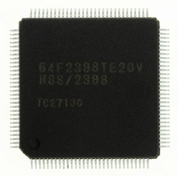
HD64F2145BTE20 Renesas Electronics America, HD64F2145BTE20 Datasheet - Page 474

HD64F2145BTE20
Manufacturer Part Number
HD64F2145BTE20
Description
IC H8S MCU FLASH 256K 100-QFP
Manufacturer
Renesas Electronics America
Series
H8® H8S/2100r
Specifications of HD64F2145BTE20
Core Processor
H8S/2000
Core Size
16-Bit
Speed
20MHz
Connectivity
I²C, IrDA, SCI, X-Bus
Peripherals
PWM, WDT
Number Of I /o
74
Program Memory Size
256KB (256K x 8)
Program Memory Type
FLASH
Ram Size
8K x 8
Voltage - Supply (vcc/vdd)
4.5 V ~ 5.5 V
Data Converters
A/D 8x10b; D/A 2x8b
Oscillator Type
Internal
Operating Temperature
-20°C ~ 75°C
Package / Case
100-TQFP, 100-VQFP
Lead Free Status / RoHS Status
Contains lead / RoHS non-compliant
Eeprom Size
-
- Current page: 474 of 847
- Download datasheet (5Mb)
Section 16 I
Reading receive data from ICDR is performed after data is transferred from ICDRS to ICDRR.
If I
transferred automatically from ICDRS to ICDRR, following reception of one frame of data using
ICDRS. If additional data is received while the ICDRF flag is 1, data is transferred automatically
from ICDRS to ICDRR by reading from ICDR. In transmit mode, no data is transferred from
ICDRS to ICDRR. Always set I
If the number of bits in a frame, excluding the acknowledge bit, is less than eight, transmit data
and receive data are stored differently. Transmit data should be written justified toward the MSB
side when MLS = 0 in ICMR, and toward the LSB side when MLS = 1. Receive data bits should
be read from the LSB side when MLS = 0, and from the MSB side when MLS = 1.
ICDR can be written to and read from only when the ICE bit is set to 1 in ICCR. The initial value
of ICDR is undefined.
16.3.2
SAR sets the slave address and selects the communication format. If the LSI is in slave mode with
the I
upper 7 bits of the first frame received after a start condition, the LSI operates as the slave device
specified by the master device. SAR can be accessed only when the ICE bit in ICCR is cleared to
0.
Bit
7
6
5
4
3
2
1
0
Rev. 3.00 Mar 21, 2006 page 418 of 788
REJ09B0300-0300
2
C is in receive mode and no previous data remains in ICDRR (the ICDRF flag is 0), data is
2
C bus format selected, when the FS bit is set to 0 and the upper 7 bits of SAR match the
Bit Name
SVA6
SVA5
SVA4
SVA3
SVA2
SVA1
SVA0
FS
Slave Address Register (SAR)
2
C Bus Interface (IIC) (Optional)
Initial Value R/W
0
0
0
0
0
0
0
0
2
C to receive mode before reading from ICDR.
R/W
R/W
R/W
R/W
R/W
R/W
R/W
R/W
Description
Slave Address 6 to 0
Set a slave address.
Format Select
Selects the communication format together with the FSX
bit in SARX and the SW bit in DDCSWR. Refer to table
16.2.
This bit should be set to 0 when general call address
recognition is performed.
Related parts for HD64F2145BTE20
Image
Part Number
Description
Manufacturer
Datasheet
Request
R

Part Number:
Description:
KIT STARTER FOR M16C/29
Manufacturer:
Renesas Electronics America
Datasheet:

Part Number:
Description:
KIT STARTER FOR R8C/2D
Manufacturer:
Renesas Electronics America
Datasheet:

Part Number:
Description:
R0K33062P STARTER KIT
Manufacturer:
Renesas Electronics America
Datasheet:

Part Number:
Description:
KIT STARTER FOR R8C/23 E8A
Manufacturer:
Renesas Electronics America
Datasheet:

Part Number:
Description:
KIT STARTER FOR R8C/25
Manufacturer:
Renesas Electronics America
Datasheet:

Part Number:
Description:
KIT STARTER H8S2456 SHARPE DSPLY
Manufacturer:
Renesas Electronics America
Datasheet:

Part Number:
Description:
KIT STARTER FOR R8C38C
Manufacturer:
Renesas Electronics America
Datasheet:

Part Number:
Description:
KIT STARTER FOR R8C35C
Manufacturer:
Renesas Electronics America
Datasheet:

Part Number:
Description:
KIT STARTER FOR R8CL3AC+LCD APPS
Manufacturer:
Renesas Electronics America
Datasheet:

Part Number:
Description:
KIT STARTER FOR RX610
Manufacturer:
Renesas Electronics America
Datasheet:

Part Number:
Description:
KIT STARTER FOR R32C/118
Manufacturer:
Renesas Electronics America
Datasheet:

Part Number:
Description:
KIT DEV RSK-R8C/26-29
Manufacturer:
Renesas Electronics America
Datasheet:

Part Number:
Description:
KIT STARTER FOR SH7124
Manufacturer:
Renesas Electronics America
Datasheet:

Part Number:
Description:
KIT STARTER FOR H8SX/1622
Manufacturer:
Renesas Electronics America
Datasheet:

Part Number:
Description:
KIT DEV FOR SH7203
Manufacturer:
Renesas Electronics America
Datasheet:


