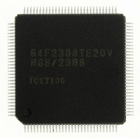
HD64F2145BTE20 Renesas Electronics America, HD64F2145BTE20 Datasheet - Page 816

HD64F2145BTE20
Manufacturer Part Number
HD64F2145BTE20
Description
IC H8S MCU FLASH 256K 100-QFP
Manufacturer
Renesas Electronics America
Series
H8® H8S/2100r
Specifications of HD64F2145BTE20
Core Processor
H8S/2000
Core Size
16-Bit
Speed
20MHz
Connectivity
I²C, IrDA, SCI, X-Bus
Peripherals
PWM, WDT
Number Of I /o
74
Program Memory Size
256KB (256K x 8)
Program Memory Type
FLASH
Ram Size
8K x 8
Voltage - Supply (vcc/vdd)
4.5 V ~ 5.5 V
Data Converters
A/D 8x10b; D/A 2x8b
Oscillator Type
Internal
Operating Temperature
-20°C ~ 75°C
Package / Case
100-TQFP, 100-VQFP
Lead Free Status / RoHS Status
Contains lead / RoHS non-compliant
Eeprom Size
-
- Current page: 816 of 847
- Download datasheet (5Mb)
Section 27 Electrical Characteristics
Notes: 1. Set the times according to the program/erase algorithms.
27.2.7
1. Internal step-down products
Rev. 3.00 Mar 21, 2006 page 760 of 788
REJ09B0300-0300
The H8S/2148 B-masked product (HD64F2148B) includes an internal step-down circuit to
step down the microprocessor internal power supply voltage to the appropriate level.
One or two (in parallel) internal voltage regulating capacitors (0.47 µF) should be inserted
between the internal step-down pin (VCL pin) and VSS pin. The method of connecting the
external capacitor(s) is shown in figure 27.5.
For the 5-V and 4-V version products whose power supply (VCC) voltage exceeds 3.6 V, do
not connect the VCC power supply to the VCL pin of the internal step-down product. (Connect
the VCC power supply to the VCC1 pin, as usual.)
For the 3-V version product whose power supply (VCC) voltage is 3.6 V or less, connect the
system power supply to the VCL pin together with the VCC1 pins.
When switching from the F-ZTAT version product without the internal step-down function to
the F-ZTAT B-masked product with the internal step-down function, note that the VCL pin is
allocated to the same location as the VCC2 pin of the product without the internal step-down
function. Therefore, the difference in the circuits between before and after the switchover
should be considered when designing the PC board patterns.
2. Programming time per 128 bytes (Shows the total period for which the P-bit in FLMCR1
3. Block erase time (Shows the total period for which the E-bit in FLMCR1 is set. It does
4. Maximum programming time (t
5. The maximun number of writes (N) should be set according to the actual set value of
6. Maximum erase time (t
7. The maximum number of erases (N) should be set according to the actual set value of z
Usage Notes
t
The wait time after P-bit setting (z1, z2, and z3) should be alternated according to the
t
is set. It does not include the programming verification time.)
not include the erase verification time.)
z1, z2 and z3 to allow programming within the maximum programming time (t
number of writes (n) as follows:
1
7
to allow erasing within the maximum erase time (t
P
E
(max) = (wait time after P-bit setting (z1) + (z3))
(max) = Wait time after E-bit setting (z)
n
n
6
1000
+ wait time after P-bit setting (z2)
z1 = 30 µs, z3 = 10 µs
z2 = 200 µs
E
(max))
P
(max))
maximum erase count (N)
((N) – 6)
E
(max)).
6
P
(max)).
Related parts for HD64F2145BTE20
Image
Part Number
Description
Manufacturer
Datasheet
Request
R

Part Number:
Description:
KIT STARTER FOR M16C/29
Manufacturer:
Renesas Electronics America
Datasheet:

Part Number:
Description:
KIT STARTER FOR R8C/2D
Manufacturer:
Renesas Electronics America
Datasheet:

Part Number:
Description:
R0K33062P STARTER KIT
Manufacturer:
Renesas Electronics America
Datasheet:

Part Number:
Description:
KIT STARTER FOR R8C/23 E8A
Manufacturer:
Renesas Electronics America
Datasheet:

Part Number:
Description:
KIT STARTER FOR R8C/25
Manufacturer:
Renesas Electronics America
Datasheet:

Part Number:
Description:
KIT STARTER H8S2456 SHARPE DSPLY
Manufacturer:
Renesas Electronics America
Datasheet:

Part Number:
Description:
KIT STARTER FOR R8C38C
Manufacturer:
Renesas Electronics America
Datasheet:

Part Number:
Description:
KIT STARTER FOR R8C35C
Manufacturer:
Renesas Electronics America
Datasheet:

Part Number:
Description:
KIT STARTER FOR R8CL3AC+LCD APPS
Manufacturer:
Renesas Electronics America
Datasheet:

Part Number:
Description:
KIT STARTER FOR RX610
Manufacturer:
Renesas Electronics America
Datasheet:

Part Number:
Description:
KIT STARTER FOR R32C/118
Manufacturer:
Renesas Electronics America
Datasheet:

Part Number:
Description:
KIT DEV RSK-R8C/26-29
Manufacturer:
Renesas Electronics America
Datasheet:

Part Number:
Description:
KIT STARTER FOR SH7124
Manufacturer:
Renesas Electronics America
Datasheet:

Part Number:
Description:
KIT STARTER FOR H8SX/1622
Manufacturer:
Renesas Electronics America
Datasheet:

Part Number:
Description:
KIT DEV FOR SH7203
Manufacturer:
Renesas Electronics America
Datasheet:


