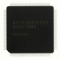
HD64F2145BTE20 Renesas Electronics America, HD64F2145BTE20 Datasheet - Page 760

HD64F2145BTE20
Manufacturer Part Number
HD64F2145BTE20
Description
IC H8S MCU FLASH 256K 100-QFP
Manufacturer
Renesas Electronics America
Series
H8® H8S/2100r
Specifications of HD64F2145BTE20
Core Processor
H8S/2000
Core Size
16-Bit
Speed
20MHz
Connectivity
I²C, IrDA, SCI, X-Bus
Peripherals
PWM, WDT
Number Of I /o
74
Program Memory Size
256KB (256K x 8)
Program Memory Type
FLASH
Ram Size
8K x 8
Voltage - Supply (vcc/vdd)
4.5 V ~ 5.5 V
Data Converters
A/D 8x10b; D/A 2x8b
Oscillator Type
Internal
Operating Temperature
-20°C ~ 75°C
Package / Case
100-TQFP, 100-VQFP
Lead Free Status / RoHS Status
Contains lead / RoHS non-compliant
Eeprom Size
-
- Current page: 760 of 847
- Download datasheet (5Mb)
Section 27 Electrical Characteristics
Notes: 1. Do not leave the AV
Rev. 3.00 Mar 21, 2006 page 704 of 788
REJ09B0300-0300
Item
Output low
voltage
2. P67 to P60 include peripheral module inputs multiplexed on those pins.
3. IRQ2 includes the ADTRG signal multiplexed on that pin.
4. P52/SCK0/SCL0, P97/SDA0, P86/SCK1/SCL1, P42/SCK2/SDA1, and port G are
5. When IICS = 0, ICE = 0, and KBIOE = 0. Low-level output when the bus drive function
6. The upper limit of the port 6 applied voltage is V
7. The upper limit of the port A applied voltage is V
8. The port A characteristics depend on V
9. For flash memory programming/erasure, the applicable range is V
Even if the A/D converter and D/A converter are not used, apply a value in the range 2.0
When the SCL0, SDA0, SCL1, or SDA1 (ICE = 1) pin is used as an output, it is NMOS
P52/SCK0, P97, P86/SCK1, P42/SCK2 (ICE = 0), and port G high levels are driven by
An external pull-up resistor is necessary to provide high-level output from SCK0, SCK1,
converter are not used.
V to 3.6 V to AV
method. Ensure that AV
NMOS push-pull outputs.
open-drain output. Therefore, an external pull-up resistor must be connected in order to
output high level.
NMOS.
and SCK2.
is selected is determined separately.
selected, and the lower of V
When a pin is in output mode, the output voltage is equivalent to the applied voltage.
selected, and the lower of V
When a pin is in output mode, the output voltage is equivalent to the applied voltage.
on V
All output pins
(except RESO) *
(Ports C to G are
added in the
H8S/2160B and
H8S/2161B.)
Ports 1 to 3
RESO
CC
.
CC
and AV
5
cc
, AV
ref
ref
ref
Symbol Min
V
pins by connection to the power supply (V
AV
OL
, and AV
CC
CC
B + 0.3 V and AV
+ 0.3 V and AV
CC
.
ss
—
—
—
pins open even if the A/D converter and D/A
CC
B, and the other pins characteristics depend
CC
CC
+ 0.3 V when CIN input is selected.
CC
CC
Typ
—
—
—
+ 0.3 V when CIN input is selected.
B + 0.3 V when CIN input is not
+ 0.3 V when CIN input is not
Max
0.4
1.0
0.4
CC
Unit
V
V
V
= 3.0 V to 3.6 V.
CC
), or some other
Test
Conditions
I
I
I
OL
OL
OL
= 1.6 mA
= 5 mA
= 1.6 mA
Related parts for HD64F2145BTE20
Image
Part Number
Description
Manufacturer
Datasheet
Request
R

Part Number:
Description:
KIT STARTER FOR M16C/29
Manufacturer:
Renesas Electronics America
Datasheet:

Part Number:
Description:
KIT STARTER FOR R8C/2D
Manufacturer:
Renesas Electronics America
Datasheet:

Part Number:
Description:
R0K33062P STARTER KIT
Manufacturer:
Renesas Electronics America
Datasheet:

Part Number:
Description:
KIT STARTER FOR R8C/23 E8A
Manufacturer:
Renesas Electronics America
Datasheet:

Part Number:
Description:
KIT STARTER FOR R8C/25
Manufacturer:
Renesas Electronics America
Datasheet:

Part Number:
Description:
KIT STARTER H8S2456 SHARPE DSPLY
Manufacturer:
Renesas Electronics America
Datasheet:

Part Number:
Description:
KIT STARTER FOR R8C38C
Manufacturer:
Renesas Electronics America
Datasheet:

Part Number:
Description:
KIT STARTER FOR R8C35C
Manufacturer:
Renesas Electronics America
Datasheet:

Part Number:
Description:
KIT STARTER FOR R8CL3AC+LCD APPS
Manufacturer:
Renesas Electronics America
Datasheet:

Part Number:
Description:
KIT STARTER FOR RX610
Manufacturer:
Renesas Electronics America
Datasheet:

Part Number:
Description:
KIT STARTER FOR R32C/118
Manufacturer:
Renesas Electronics America
Datasheet:

Part Number:
Description:
KIT DEV RSK-R8C/26-29
Manufacturer:
Renesas Electronics America
Datasheet:

Part Number:
Description:
KIT STARTER FOR SH7124
Manufacturer:
Renesas Electronics America
Datasheet:

Part Number:
Description:
KIT STARTER FOR H8SX/1622
Manufacturer:
Renesas Electronics America
Datasheet:

Part Number:
Description:
KIT DEV FOR SH7203
Manufacturer:
Renesas Electronics America
Datasheet:


