HD64F2145BTE20 Renesas Electronics America, HD64F2145BTE20 Datasheet - Page 31
HD64F2145BTE20
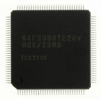
Manufacturer Part Number
HD64F2145BTE20
Description
IC H8S MCU FLASH 256K 100-QFP
Manufacturer
Renesas Electronics America
Series
H8® H8S/2100r
Specifications of HD64F2145BTE20
Core Processor
H8S/2000
Core Size
16-Bit
Speed
20MHz
Connectivity
I²C, IrDA, SCI, X-Bus
Peripherals
PWM, WDT
Number Of I /o
74
Program Memory Size
256KB (256K x 8)
Program Memory Type
FLASH
Ram Size
8K x 8
Voltage - Supply (vcc/vdd)
4.5 V ~ 5.5 V
Data Converters
A/D 8x10b; D/A 2x8b
Oscillator Type
Internal
Operating Temperature
-20°C ~ 75°C
Package / Case
100-TQFP, 100-VQFP
Lead Free Status / RoHS Status
Contains lead / RoHS non-compliant
Eeprom Size
-


12.7 Input Capture Operation.................................................................................................... 306
12.8 Interrupt Sources............................................................................................................... 309
12.9 Usage Notes ...................................................................................................................... 310
Section 13 Timer Connection
13.1 Features ............................................................................................................................. 317
13.2 Input/Output Pins .............................................................................................................. 319
13.3 Register Descriptions ........................................................................................................ 319
13.4 Operation .......................................................................................................................... 329
13.5 Usage Note........................................................................................................................ 344
Section 14 Watchdog Timer (WDT)
14.1 Features ............................................................................................................................. 345
14.2 Input/Output Pins .............................................................................................................. 347
14.3 Register Descriptions ........................................................................................................ 347
12.6.1 16-Bit Count Mode .............................................................................................. 305
12.6.2 Compare-Match Count Mode .............................................................................. 306
12.9.1 Conflict between TCNT Write and Clear ............................................................ 310
12.9.2 Conflict between TCNT Write and Increment..................................................... 311
12.9.3 Conflict between TCOR Write and Compare-Match........................................... 312
12.9.4 Conflict between Compare-Matches A and B...................................................... 313
12.9.5 Switching of Internal Clocks and TCNT Operation............................................. 313
12.9.6 Mode Setting with Cascaded Connection ............................................................ 315
12.9.7 Module Stop Mode Setting .................................................................................. 315
13.3.1 Timer Connection Register I (TCONRI) ............................................................. 320
13.3.2 Timer Connection Register O (TCONRO) .......................................................... 323
13.3.3 Timer Connection Register S (TCONRS)............................................................ 325
13.3.4 Edge Sense Register (SEDGR) ............................................................................ 327
13.4.1 PWM Decoding (PDC Signal Generation) .......................................................... 329
13.4.2 Clamp Waveform Generation (CL1/CL2/CL3 Signal Generation) ..................... 330
13.4.3 Measurement of 8-Bit Timer Divided Waveform Period .................................... 332
13.4.4 2fH Modification of IHI Signal ........................................................................... 334
13.4.5 IVI Signal Fall Modification and IHI Synchronization ....................................... 336
13.4.6 Internal Synchronization Signal Generation (IHG/IVG/CL4 Signal
13.4.7 HSYNCO Output ................................................................................................. 341
13.4.8 VSYNCO Output ................................................................................................. 342
13.4.9 CBLANK Output ................................................................................................. 343
13.5.1 Module Stop Mode Setting .................................................................................. 344
14.3.1 Timer Counter (TCNT)........................................................................................ 347
14.3.2 Timer Control/Status Register (TCSR) ................................................................ 348
Generation) .......................................................................................................... 338
........................................................................................... 317
.............................................................................. 345
Rev. 3.00 Mar 21, 2006 page xxix of liv
Related parts for HD64F2145BTE20
Image
Part Number
Description
Manufacturer
Datasheet
Request
R

Part Number:
Description:
KIT STARTER FOR M16C/29
Manufacturer:
Renesas Electronics America
Datasheet:

Part Number:
Description:
KIT STARTER FOR R8C/2D
Manufacturer:
Renesas Electronics America
Datasheet:

Part Number:
Description:
R0K33062P STARTER KIT
Manufacturer:
Renesas Electronics America
Datasheet:

Part Number:
Description:
KIT STARTER FOR R8C/23 E8A
Manufacturer:
Renesas Electronics America
Datasheet:

Part Number:
Description:
KIT STARTER FOR R8C/25
Manufacturer:
Renesas Electronics America
Datasheet:

Part Number:
Description:
KIT STARTER H8S2456 SHARPE DSPLY
Manufacturer:
Renesas Electronics America
Datasheet:

Part Number:
Description:
KIT STARTER FOR R8C38C
Manufacturer:
Renesas Electronics America
Datasheet:

Part Number:
Description:
KIT STARTER FOR R8C35C
Manufacturer:
Renesas Electronics America
Datasheet:

Part Number:
Description:
KIT STARTER FOR R8CL3AC+LCD APPS
Manufacturer:
Renesas Electronics America
Datasheet:
Part Number:
Description:
KIT STARTER FOR RX610
Manufacturer:
Renesas Electronics America
Datasheet:

Part Number:
Description:
KIT STARTER FOR R32C/118
Manufacturer:
Renesas Electronics America
Datasheet:

Part Number:
Description:
KIT DEV RSK-R8C/26-29
Manufacturer:
Renesas Electronics America
Datasheet:

Part Number:
Description:
KIT STARTER FOR SH7124
Manufacturer:
Renesas Electronics America
Datasheet:

Part Number:
Description:
KIT STARTER FOR H8SX/1622
Manufacturer:
Renesas Electronics America
Datasheet:

Part Number:
Description:
KIT DEV FOR SH7203
Manufacturer:
Renesas Electronics America
Datasheet: