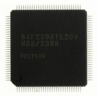
HD64F2145BTE20 Renesas Electronics America, HD64F2145BTE20 Datasheet - Page 300

HD64F2145BTE20
Manufacturer Part Number
HD64F2145BTE20
Description
IC H8S MCU FLASH 256K 100-QFP
Manufacturer
Renesas Electronics America
Series
H8® H8S/2100r
Specifications of HD64F2145BTE20
Core Processor
H8S/2000
Core Size
16-Bit
Speed
20MHz
Connectivity
I²C, IrDA, SCI, X-Bus
Peripherals
PWM, WDT
Number Of I /o
74
Program Memory Size
256KB (256K x 8)
Program Memory Type
FLASH
Ram Size
8K x 8
Voltage - Supply (vcc/vdd)
4.5 V ~ 5.5 V
Data Converters
A/D 8x10b; D/A 2x8b
Oscillator Type
Internal
Operating Temperature
-20°C ~ 75°C
Package / Case
100-TQFP, 100-VQFP
Lead Free Status / RoHS Status
Contains lead / RoHS non-compliant
Eeprom Size
-
- Current page: 300 of 847
- Download datasheet (5Mb)
Section 10 14-Bit PWM Timer (PWMX)
10.2
Table 10.1 lists the PWM (D/A) module input and output pins.
Table 10.1 Pin Configuration
Name
PWM output pin X0
PWM output pin X1
10.3
The PWM (D/A) module has the following registers. The PWM (D/A) registers are assigned to the
same addresses with other registers. The registers are selected by the IICE bit in the serial timer
control register (STCR). For details on STCR, see section 3.2.3, Serial Timer Control Register
(STCR).
Note: The same addresses are shared by DADRA and DACR, and by DADRB and DACNT.
Rev. 3.00 Mar 21, 2006 page 244 of 788
REJ09B0300-0300
PWM (D/A) counter H (DACNTH)
PWM (D/A) counter L (DACNTL)
PWM (D/A) data register AH (DADRAH)
PWM (D/A) data register AL (DADRAL)
PWM (D/A) data register BH (DADRBH)
PWM (D/A) data register BL (DADRBL)
PWM (D/A) control register (DACR)
Switching is performed by the REGS bit in DACNT or DADRB.
Register Descriptions
Input/Output Pins
Abbreviation
PWX0
PWX1
I/O
Output
Output
Function
PWM output of PWMX channel A
PWM output of PWMX channel B
Related parts for HD64F2145BTE20
Image
Part Number
Description
Manufacturer
Datasheet
Request
R

Part Number:
Description:
KIT STARTER FOR M16C/29
Manufacturer:
Renesas Electronics America
Datasheet:

Part Number:
Description:
KIT STARTER FOR R8C/2D
Manufacturer:
Renesas Electronics America
Datasheet:

Part Number:
Description:
R0K33062P STARTER KIT
Manufacturer:
Renesas Electronics America
Datasheet:

Part Number:
Description:
KIT STARTER FOR R8C/23 E8A
Manufacturer:
Renesas Electronics America
Datasheet:

Part Number:
Description:
KIT STARTER FOR R8C/25
Manufacturer:
Renesas Electronics America
Datasheet:

Part Number:
Description:
KIT STARTER H8S2456 SHARPE DSPLY
Manufacturer:
Renesas Electronics America
Datasheet:

Part Number:
Description:
KIT STARTER FOR R8C38C
Manufacturer:
Renesas Electronics America
Datasheet:

Part Number:
Description:
KIT STARTER FOR R8C35C
Manufacturer:
Renesas Electronics America
Datasheet:

Part Number:
Description:
KIT STARTER FOR R8CL3AC+LCD APPS
Manufacturer:
Renesas Electronics America
Datasheet:

Part Number:
Description:
KIT STARTER FOR RX610
Manufacturer:
Renesas Electronics America
Datasheet:

Part Number:
Description:
KIT STARTER FOR R32C/118
Manufacturer:
Renesas Electronics America
Datasheet:

Part Number:
Description:
KIT DEV RSK-R8C/26-29
Manufacturer:
Renesas Electronics America
Datasheet:

Part Number:
Description:
KIT STARTER FOR SH7124
Manufacturer:
Renesas Electronics America
Datasheet:

Part Number:
Description:
KIT STARTER FOR H8SX/1622
Manufacturer:
Renesas Electronics America
Datasheet:

Part Number:
Description:
KIT DEV FOR SH7203
Manufacturer:
Renesas Electronics America
Datasheet:


