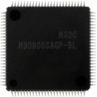
M30800SAGP-BL#U5 Renesas Electronics America, M30800SAGP-BL#U5 Datasheet - Page 182

M30800SAGP-BL#U5
Manufacturer Part Number
M30800SAGP-BL#U5
Description
IC M32C/80 MCU ROMLESS 100LQFP
Manufacturer
Renesas Electronics America
Series
M16C™ M32C/80r
Datasheet
1.M30800SAGP-BLU5.pdf
(354 pages)
Specifications of M30800SAGP-BL#U5
Core Processor
M16C/80
Core Size
16-Bit
Speed
20MHz
Connectivity
I²C, IEBus, SIO, UART/USART
Peripherals
DMA, WDT
Number Of I /o
45
Program Memory Type
ROMless
Ram Size
8K x 8
Voltage - Supply (vcc/vdd)
3 V ~ 5.5 V
Data Converters
A/D 10x10b, D/A 2x8b
Oscillator Type
Internal
Operating Temperature
-20°C ~ 85°C
Package / Case
100-LQFP
For Use With
R0K330879S001BE - KIT DEV RSK M32C/87R0K330879S000BE - KIT DEV RSK M32C/87
Lead Free Status / RoHS Status
Lead free / RoHS Compliant
Eeprom Size
-
Program Memory Size
-
Available stocks
Company
Part Number
Manufacturer
Quantity
Price
- Current page: 182 of 354
- Download datasheet (3Mb)
M
R
R
e
E
3
. v
J
2
Figure 15.4 IDB0 and IDB1 registers, DTT Register
0
C
1
9
0 .
8 /
B
0
0
0
2
7
G
N
1
o
o r
0 -
b7
Dead Time Timer
Three-Phase Output Buffer Register i
. v
b7
NOTE:
u
NOTES:
1
0
p
0
1. Values of the IDB0 and IDB1 registers are transferred to the three-phase output shift register by a
b6
, 1
1. Use the MOV instruction to set the DTT register.
2. The DTT register setting is enabled when the INV15 bit in the INVC1 register is set to "0" (dead time
0
transfer trigger.
signal level first. Then the value written in the IDB1 register on the falling edge of the timers A1, A2
and A4 one-shot pulse determines each phase output signal level.
After the transfer trigger occurs, the values written in the IDB0 register determine each phase output
enabled). No dead time can be set when the INV15 bit is set to "1" (dead time disabled). The INV06
bit in the INVC0 register determines start trigger of the DTT register.
2
b5
0
0
b4
5
Page 161
b3
b2
b1
b0
b0
(1, 2)
f o
(b7 - b6)
If setting value is n, the timer stops when counting
n times a count source selected by the INV12 bit
after start trigger occurs. Positive or negative
phase, which changes from inactive level to active
level, shifts when the dead time timer stops.
3
Symbol
DWBi
DUBi
DVBi
DWi
3
DUi
DVi
Bit
0
Symbol
DTT
Symbol
IDB0, IDB1
U-Phase Output Buffer i
U-Phase Output Buffer i
V-Phase Output Buffer i
V-Phase Output Buffer i
W-Phase Output Buffer i
W-Phase Output Buffer i
Reserved Bit
Bit Name
Function
Address
030C
Address
030A
16
16
(1) (i=0, 1)
, 030B
15. Three-Phase Motor Control Timer Functions
16
Write output level
0: Active level
1: Inactive level
When read, the value of the three-
phase shift register is read.
When read,
its content is indeterminate
Function
After Reset
XX11 1111
Setting Range
After Reset
Indeterminate
1 to 255
2
RW
RW
RW
RW
RW
RW
RW
RO
RW
WO
Related parts for M30800SAGP-BL#U5
Image
Part Number
Description
Manufacturer
Datasheet
Request
R

Part Number:
Description:
IC M32C/80 MCU ROMLESS 100LQFP
Manufacturer:
Renesas Electronics America
Datasheet:

Part Number:
Description:
IC M16C MPU ROMLESS 100LQFP
Manufacturer:
Renesas Electronics America
Datasheet:

Part Number:
Description:
MCU 3/5V 0K I-TEMP 100-LQFP
Manufacturer:
Renesas Electronics America
Datasheet:

Part Number:
Description:
KIT STARTER FOR M16C/29
Manufacturer:
Renesas Electronics America
Datasheet:

Part Number:
Description:
KIT STARTER FOR R8C/2D
Manufacturer:
Renesas Electronics America
Datasheet:

Part Number:
Description:
R0K33062P STARTER KIT
Manufacturer:
Renesas Electronics America
Datasheet:

Part Number:
Description:
KIT STARTER FOR R8C/23 E8A
Manufacturer:
Renesas Electronics America
Datasheet:

Part Number:
Description:
KIT STARTER FOR R8C/25
Manufacturer:
Renesas Electronics America
Datasheet:

Part Number:
Description:
KIT STARTER H8S2456 SHARPE DSPLY
Manufacturer:
Renesas Electronics America
Datasheet:

Part Number:
Description:
KIT STARTER FOR R8C38C
Manufacturer:
Renesas Electronics America
Datasheet:

Part Number:
Description:
KIT STARTER FOR R8C35C
Manufacturer:
Renesas Electronics America
Datasheet:

Part Number:
Description:
KIT STARTER FOR R8CL3AC+LCD APPS
Manufacturer:
Renesas Electronics America
Datasheet:

Part Number:
Description:
KIT STARTER FOR RX610
Manufacturer:
Renesas Electronics America
Datasheet:

Part Number:
Description:
KIT STARTER FOR R32C/118
Manufacturer:
Renesas Electronics America
Datasheet:

Part Number:
Description:
KIT DEV RSK-R8C/26-29
Manufacturer:
Renesas Electronics America
Datasheet:


