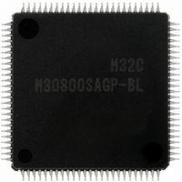
M30800SAGP-BL#U5 Renesas Electronics America, M30800SAGP-BL#U5 Datasheet - Page 195

M30800SAGP-BL#U5
Manufacturer Part Number
M30800SAGP-BL#U5
Description
IC M32C/80 MCU ROMLESS 100LQFP
Manufacturer
Renesas Electronics America
Series
M16C™ M32C/80r
Datasheet
1.M30800SAGP-BLU5.pdf
(354 pages)
Specifications of M30800SAGP-BL#U5
Core Processor
M16C/80
Core Size
16-Bit
Speed
20MHz
Connectivity
I²C, IEBus, SIO, UART/USART
Peripherals
DMA, WDT
Number Of I /o
45
Program Memory Type
ROMless
Ram Size
8K x 8
Voltage - Supply (vcc/vdd)
3 V ~ 5.5 V
Data Converters
A/D 10x10b, D/A 2x8b
Oscillator Type
Internal
Operating Temperature
-20°C ~ 85°C
Package / Case
100-LQFP
For Use With
R0K330879S001BE - KIT DEV RSK M32C/87R0K330879S000BE - KIT DEV RSK M32C/87
Lead Free Status / RoHS Status
Lead free / RoHS Compliant
Eeprom Size
-
Program Memory Size
-
Available stocks
Company
Part Number
Manufacturer
Quantity
Price
- Current page: 195 of 354
- Download datasheet (3Mb)
M
R
R
e
E
3
. v
J
2
Figure 16.7 U0SMR3 to U4SMR3 Registers
0
C
1
9
0 .
8 /
B
0
0
0
2
7
G
N
1
o
o r
UARTi Special Mode Register 3
0 -
b7
. v
NOTES:
u
1
p
0
0
b6
1. Set the SS pin after the CRD bit in the UiC0 register is set to "1" (CTS/RTS function disabled).
2. The ERR bit is set to "0" by program. It is unchanged if set to "1".
3. Digital delay is generated from a SDAi output by the DL2 to DL0 bits in I
4. When the external clock is selected, approximately 100ns delay is added.
, 1
0
"000
b5
2
0
0
b4
2
5
" (no delay) except in the I
b3
Page 174
b2
b1
b0
f o
Symbol
NODC
CKPH
3
DINC
ERR
SSE
DL0
DL1
DL2
3
Bit
0
Symbol
U0SMR3 to U4SMR3
2
C mode.
SS Pin Function
Enable Bit
Clock Phase
Set Bit
Serial Input Port
Set Bit
Clock Output
Select Bit
Fault Error Flag
SDAi Digital Delay
Time Set Bit
Bit Name
(1)
(i=0 to 4)
(3, 4)
(2)
Address
0365
16,
b7 b6 b5
0: Disables SS pin function
1: Enables SS pin function
0: No clock delay
1: Clock delay
0: Selects the TxDi and RxDi pins
1: Selects the STxDi and SRxDi pins
0: CMOS output
1: N-channel open drain output
0: No error
1: Error
0 0 0: No delay
0 0 1: 1-to-2 cycles of BRG count source
0 1 0: 2-to-3 cycles of BRG count source
0 1 1: 3-to-4 cycles of BRG count source
1 0 0: 4-to-5 cycles of BRG count source
1 0 1: 5-to-6 cycles of BRG count source
1 1 0: 6-to-7 cycles of BRG count source
1 1 1: 7-to-8 cycles of BRG count source
02E5
(master mode)
(slave mode)
16,
0335
16,
0325
2
C mode. Set these bits to
Function
16,
02F5
16
After Reset
00
16
RW
RW
RW
RW
RW
RW
RW
RW
RW
16. Serial I/O
Related parts for M30800SAGP-BL#U5
Image
Part Number
Description
Manufacturer
Datasheet
Request
R

Part Number:
Description:
IC M32C/80 MCU ROMLESS 100LQFP
Manufacturer:
Renesas Electronics America
Datasheet:

Part Number:
Description:
IC M16C MPU ROMLESS 100LQFP
Manufacturer:
Renesas Electronics America
Datasheet:

Part Number:
Description:
MCU 3/5V 0K I-TEMP 100-LQFP
Manufacturer:
Renesas Electronics America
Datasheet:

Part Number:
Description:
KIT STARTER FOR M16C/29
Manufacturer:
Renesas Electronics America
Datasheet:

Part Number:
Description:
KIT STARTER FOR R8C/2D
Manufacturer:
Renesas Electronics America
Datasheet:

Part Number:
Description:
R0K33062P STARTER KIT
Manufacturer:
Renesas Electronics America
Datasheet:

Part Number:
Description:
KIT STARTER FOR R8C/23 E8A
Manufacturer:
Renesas Electronics America
Datasheet:

Part Number:
Description:
KIT STARTER FOR R8C/25
Manufacturer:
Renesas Electronics America
Datasheet:

Part Number:
Description:
KIT STARTER H8S2456 SHARPE DSPLY
Manufacturer:
Renesas Electronics America
Datasheet:

Part Number:
Description:
KIT STARTER FOR R8C38C
Manufacturer:
Renesas Electronics America
Datasheet:

Part Number:
Description:
KIT STARTER FOR R8C35C
Manufacturer:
Renesas Electronics America
Datasheet:

Part Number:
Description:
KIT STARTER FOR R8CL3AC+LCD APPS
Manufacturer:
Renesas Electronics America
Datasheet:

Part Number:
Description:
KIT STARTER FOR RX610
Manufacturer:
Renesas Electronics America
Datasheet:

Part Number:
Description:
KIT STARTER FOR R32C/118
Manufacturer:
Renesas Electronics America
Datasheet:

Part Number:
Description:
KIT DEV RSK-R8C/26-29
Manufacturer:
Renesas Electronics America
Datasheet:


