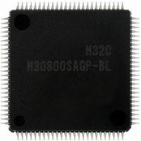
M30800SAGP-BL#U5 Renesas Electronics America, M30800SAGP-BL#U5 Datasheet - Page 32

M30800SAGP-BL#U5
Manufacturer Part Number
M30800SAGP-BL#U5
Description
IC M32C/80 MCU ROMLESS 100LQFP
Manufacturer
Renesas Electronics America
Series
M16C™ M32C/80r
Datasheet
1.M30800SAGP-BLU5.pdf
(354 pages)
Specifications of M30800SAGP-BL#U5
Core Processor
M16C/80
Core Size
16-Bit
Speed
20MHz
Connectivity
I²C, IEBus, SIO, UART/USART
Peripherals
DMA, WDT
Number Of I /o
45
Program Memory Type
ROMless
Ram Size
8K x 8
Voltage - Supply (vcc/vdd)
3 V ~ 5.5 V
Data Converters
A/D 10x10b, D/A 2x8b
Oscillator Type
Internal
Operating Temperature
-20°C ~ 85°C
Package / Case
100-LQFP
For Use With
R0K330879S001BE - KIT DEV RSK M32C/87R0K330879S000BE - KIT DEV RSK M32C/87
Lead Free Status / RoHS Status
Lead free / RoHS Compliant
Eeprom Size
-
Program Memory Size
-
Available stocks
Company
Part Number
Manufacturer
Quantity
Price
- Current page: 32 of 354
- Download datasheet (3Mb)
M
R
R
e
E
3
. v
J
2
Table 1.5 Pin Description (Continued)
I: Input
NOTES:
0
Reference
voltage input
A/D converter
D/A converter
Intelligent I/O
communication
function
I/O port
C
1
9
Signal name
8 /
0 .
B
1. Ports P0 to P5 function as bus control pins when using memory expansion mode or microprocessor mode. They
2. Port P1 functions as I/O port when the microcomputer is placed in memory expansion mode or microprocessor
0
0
0
2
cannot be used as I/O ports.
mode and all external data buses are selected as 8-bit buses.
G
7
N
1
o r
o
0 -
. v
u
O: Output
1
p
0
0
, 1
0
2
0
V
AN
AD
ANEX0
ANEX1
DA0, DA1
ISCLK0
ISCLK1
ISTxD0
ISTxD1
ISRxD0
ISRxD1
P0
P1
P2
P3
P4
P5
P6
P7
P9
P10
P8
P8
P8
___________
Pin name I/O type
0
REF
5
0
0
0
0
0
0
0
0
0
0
6
5
0
TRG
0
, P8
to P0
to P1
to P2
to P3
to P4
to P5
to P6
to P7
to P9
to P8
to AN
to P10
page 11
7
I/O: Input and output
7 (1)
7 (2)
7 (1)
7 (1)
7 (1)
7 (1)
7
7
7
4
,
7
7
I/O
I/O
I/O
I/O
I/O
O
O
f o
I
I
I
I
I
I
3
3
0
voltage
V
V
V
V
V
V
V
V
V
V
V
V
Supply
CC1
CC1
CC1
CC1
CC1
CC1
CC1
CC1
CC2
CC1
CC1
CC1
-
Applies reference voltage for the A/D converter and D/A converter
Analog input pins for the A/D converter
Input pin for an external A/D trigger
Extended analog input pin for the A/D converter and output pin in
external op-amp connection mode
Extended analog input pin for the A/D converter
Output pin for the D/A converter
Inputs and outputs clock for the intelligent I/O communication
fucntion
Outputs data for the intelligent I/O communication fucntion
Inputs data for the intelligent I/O communication fucntion
I/O ports fro CMOS. Each port can be programmed for nput or
output under the control of the direction register. An input port
can be set, by program, for a pull-up resistor available or for no
pull-up resistor available in 4-bit units
I/O ports having equivalent functions to P0
(P7
I/O ports having equivalent functions to P0
Shares a pin with NMI. NMI input state can be got by reading P8
0
and P7
1
are ports for the N-channel open drain output.)
_______
_______
Description
1. Overview
5
Related parts for M30800SAGP-BL#U5
Image
Part Number
Description
Manufacturer
Datasheet
Request
R

Part Number:
Description:
IC M32C/80 MCU ROMLESS 100LQFP
Manufacturer:
Renesas Electronics America
Datasheet:

Part Number:
Description:
IC M16C MPU ROMLESS 100LQFP
Manufacturer:
Renesas Electronics America
Datasheet:

Part Number:
Description:
MCU 3/5V 0K I-TEMP 100-LQFP
Manufacturer:
Renesas Electronics America
Datasheet:

Part Number:
Description:
KIT STARTER FOR M16C/29
Manufacturer:
Renesas Electronics America
Datasheet:

Part Number:
Description:
KIT STARTER FOR R8C/2D
Manufacturer:
Renesas Electronics America
Datasheet:

Part Number:
Description:
R0K33062P STARTER KIT
Manufacturer:
Renesas Electronics America
Datasheet:

Part Number:
Description:
KIT STARTER FOR R8C/23 E8A
Manufacturer:
Renesas Electronics America
Datasheet:

Part Number:
Description:
KIT STARTER FOR R8C/25
Manufacturer:
Renesas Electronics America
Datasheet:

Part Number:
Description:
KIT STARTER H8S2456 SHARPE DSPLY
Manufacturer:
Renesas Electronics America
Datasheet:

Part Number:
Description:
KIT STARTER FOR R8C38C
Manufacturer:
Renesas Electronics America
Datasheet:

Part Number:
Description:
KIT STARTER FOR R8C35C
Manufacturer:
Renesas Electronics America
Datasheet:

Part Number:
Description:
KIT STARTER FOR R8CL3AC+LCD APPS
Manufacturer:
Renesas Electronics America
Datasheet:

Part Number:
Description:
KIT STARTER FOR RX610
Manufacturer:
Renesas Electronics America
Datasheet:

Part Number:
Description:
KIT STARTER FOR R32C/118
Manufacturer:
Renesas Electronics America
Datasheet:

Part Number:
Description:
KIT DEV RSK-R8C/26-29
Manufacturer:
Renesas Electronics America
Datasheet:


