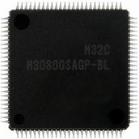
M30800SAGP-BL#U5 Renesas Electronics America, M30800SAGP-BL#U5 Datasheet - Page 244

M30800SAGP-BL#U5
Manufacturer Part Number
M30800SAGP-BL#U5
Description
IC M32C/80 MCU ROMLESS 100LQFP
Manufacturer
Renesas Electronics America
Series
M16C™ M32C/80r
Datasheet
1.M30800SAGP-BLU5.pdf
(354 pages)
Specifications of M30800SAGP-BL#U5
Core Processor
M16C/80
Core Size
16-Bit
Speed
20MHz
Connectivity
I²C, IEBus, SIO, UART/USART
Peripherals
DMA, WDT
Number Of I /o
45
Program Memory Type
ROMless
Ram Size
8K x 8
Voltage - Supply (vcc/vdd)
3 V ~ 5.5 V
Data Converters
A/D 10x10b, D/A 2x8b
Oscillator Type
Internal
Operating Temperature
-20°C ~ 85°C
Package / Case
100-LQFP
For Use With
R0K330879S001BE - KIT DEV RSK M32C/87R0K330879S000BE - KIT DEV RSK M32C/87
Lead Free Status / RoHS Status
Lead free / RoHS Compliant
Eeprom Size
-
Program Memory Size
-
Available stocks
Company
Part Number
Manufacturer
Quantity
Price
- Current page: 244 of 354
- Download datasheet (3Mb)
M
R
R
e
E
3
. v
J
2
Figure 17.3 AD0CON1 Register
0
C
1
9
8 /
0 .
B
0
0
0
2
G
7
N
1
o r
o
0 -
A/D0 Control Register 1
. v
b7
u
NOTES:
1
p
0
0
b6
, 1
1. When the AD0CON1 register is rewritten during the A/D conversion, the conversion result is
2. The SCAN1 and SCAN0 bit settings are disabled in repeat sweep mode 1.
3. This pin is commonly used in the A/D conversion when the MD2 bit is set to "1".
4. Refer to the note for the CKS0 bit in the AD0CON0 register.
5. In one-shot mode and repeat mode, the OPA1 and OPA0 bits can be set to "01
6. To set the OPA1 and OPA0 bits to "00
7. AV
8. Do not set the VCUT bit to "0" during the A/D conversion.
0
2
indeterminate.
set the OPA0 and OPA1 bits to "01
ANEX0) and the PSL3_6 bit to "0" (other than ANEX1).
V
of the D/A converter.
b5
0
REF
CC
0
b4
5
=V
is a reference voltage for AD0 only. The VCUT bit setting does not affect the V
b3
Page 223
REF
b2
=V
CC1
b1
, AD input voltage (for AN
b0
f o
Symbol
SCAN0
SCAN1
3
VCUT
CKS1
OPA0
OPA1
MD2
BITS
3
Bit
0
Symbol
AD0CON1
(1)
A/D Sweep Pin
Select Bit
A/D Operating
Mode Select Bit 1
8/10-Bit Mode
Select Bit
Frequency Select
Bit
V
Bit
External Op-Amp
Connection Mode
Bit
REF
2
(5)
" or "10
Bit Name
2
Connection
", set the PSL3_5 bit in PSL3 register to "0" (other than
(2, 7)
0
2
Address
0397
" in other modes.
to AN
16
7
, ANEX0, ANEX1)
b7
Single sweep mode and repeat sweep mode 0
Repeat sweep mode 1
0: Any mode other than repeat sweep mode 1
1: Repeat sweep mode 1
0: 8-bit mode
1: 10-bit mode
0: No V
1: V
0 0: ANEX0 and ANEX1 are not used
0 1: Signal into ANEX0 is A/D converted
1 0: Signal into ANEX1 is A/D converted
1 1: External op-amp connection mode
(Note 4)
b1
0 0: AN
0 1: AN
1 0: AN
1 1: AN
0 0: AN
0 1: AN
1 0: AN
1 1: AN
b1
b6
b0
b0
REF
REF
connection
0
0
0
0
0
0
0
0
, AN
, AN
to AN
to AN
to AN
to AN
to AN
connection
1
1
3
5
7
2
3
Function
After Reset
00
V
CC1
16
(3)
(8)
.
2
" or "10
REF
2
" only. Do not
performance
(6)
17. A/D Converter
RW
RW
RW
RW
RW
RW
RW
RW
RW
Related parts for M30800SAGP-BL#U5
Image
Part Number
Description
Manufacturer
Datasheet
Request
R

Part Number:
Description:
IC M32C/80 MCU ROMLESS 100LQFP
Manufacturer:
Renesas Electronics America
Datasheet:

Part Number:
Description:
IC M16C MPU ROMLESS 100LQFP
Manufacturer:
Renesas Electronics America
Datasheet:

Part Number:
Description:
MCU 3/5V 0K I-TEMP 100-LQFP
Manufacturer:
Renesas Electronics America
Datasheet:

Part Number:
Description:
KIT STARTER FOR M16C/29
Manufacturer:
Renesas Electronics America
Datasheet:

Part Number:
Description:
KIT STARTER FOR R8C/2D
Manufacturer:
Renesas Electronics America
Datasheet:

Part Number:
Description:
R0K33062P STARTER KIT
Manufacturer:
Renesas Electronics America
Datasheet:

Part Number:
Description:
KIT STARTER FOR R8C/23 E8A
Manufacturer:
Renesas Electronics America
Datasheet:

Part Number:
Description:
KIT STARTER FOR R8C/25
Manufacturer:
Renesas Electronics America
Datasheet:

Part Number:
Description:
KIT STARTER H8S2456 SHARPE DSPLY
Manufacturer:
Renesas Electronics America
Datasheet:

Part Number:
Description:
KIT STARTER FOR R8C38C
Manufacturer:
Renesas Electronics America
Datasheet:

Part Number:
Description:
KIT STARTER FOR R8C35C
Manufacturer:
Renesas Electronics America
Datasheet:

Part Number:
Description:
KIT STARTER FOR R8CL3AC+LCD APPS
Manufacturer:
Renesas Electronics America
Datasheet:

Part Number:
Description:
KIT STARTER FOR RX610
Manufacturer:
Renesas Electronics America
Datasheet:

Part Number:
Description:
KIT STARTER FOR R32C/118
Manufacturer:
Renesas Electronics America
Datasheet:

Part Number:
Description:
KIT DEV RSK-R8C/26-29
Manufacturer:
Renesas Electronics America
Datasheet:


