ATEVK1104 Atmel, ATEVK1104 Datasheet - Page 526
ATEVK1104
Manufacturer Part Number
ATEVK1104
Description
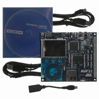
KIT DEV/EVAL FOR AVR32 AT32UC3A
Manufacturer
Atmel
Series
AVR®32r
Type
MCUr
Datasheets
1.ATAVRONE-PROBECBL.pdf
(16 pages)
2.ATEVK1104.pdf
(826 pages)
3.ATEVK1104.pdf
(90 pages)
4.ATEVK1104.pdf
(6 pages)
5.ATEVK1104.pdf
(12 pages)
Specifications of ATEVK1104
Contents
Evaluation Board, Software and Documentation
Processor To Be Evaluated
AT32UC3A3
Data Bus Width
32 bit
Interface Type
USB, SPI, USART
Silicon Manufacturer
Atmel
Core Architecture
AVR
Core Sub-architecture
AVR UC3
Silicon Core Number
AT32UC3A3256
Silicon Family Name
AVR
Kit Contents
Board CD Docs
Rohs Compliant
Yes
For Use With/related Products
AT32UC3A3
Lead Free Status / RoHS Status
Lead free / RoHS Compliant
Available stocks
Company
Part Number
Manufacturer
Quantity
Price
Company:

Part Number:
ATEVK1104
Manufacturer:
Atmel
Quantity:
135


Figure 30-25. Example of an IN Pipe with 1 Data Bank
Figure 30-26. Example of an IN Pipe with 2 Data Banks
30.7.3.11
32058J–AVR32–04/11
RXINI
FIFOCON
IN
Management of OUT Pipes
RXINI
FIFOCON
(bank 0)
IN
DATA
OUT packets are sent by the host. All the data can be written by the firmware which acknowl-
edges or not the bank when it is full.
The pipe must be configured and unfrozen first.
The TXOUTI bit is set by hardware at the same time as FIFOCON when the current bank is free.
This triggers a PXINT interrupt if TXOUTE = 1.
TXOUTI shall be cleared by software (by setting the TXOUTIC bit) to acknowledge the interrupt,
what has no effect on the pipe FIFO.
The firmware then writes into the FIFO and clears the FIFOCON bit to allow the USB controller
to send the data. If the OUT pipe is composed of multiple banks, this also switches to the next
bank. The TXOUTI and FIFOCON bits are updated by hardware in accordance with the status of
the next bank.
TXOUTI shall always be cleared before clearing FIFOCON.
The RWALL bit is set by hardware when the current bank is not full, i.e. the software can write
further data into the FIFO.
Note that if the firmware decides to switch to the Suspend state (by clearing the SOFE bit) while
a bank is ready to be sent, the USB controller automatically exits this state and the bank is sent.
(bank 0)
DATA
HW
ACK
SW
read data from CPU
HW
ACK
BANK 0
SW
read data from CPU
IN
BANK 0
SW
(bank 1)
IN
DATA
SW
(bank 0)
DATA
HW
ACK
read data from CPU
SW
HW
ACK
BANK 1
read data from CPU
AT32UC3A
SW
BANK 0
526
Related parts for ATEVK1104
Image
Part Number
Description
Manufacturer
Datasheet
Request
R

Part Number:
Description:
DEV KIT FOR AVR/AVR32
Manufacturer:
Atmel
Datasheet:

Part Number:
Description:
INTERVAL AND WIPE/WASH WIPER CONTROL IC WITH DELAY
Manufacturer:
ATMEL Corporation
Datasheet:
Part Number:
Description:
Low-Voltage Voice-Switched IC for Hands-Free Operation
Manufacturer:
ATMEL Corporation
Datasheet:
Part Number:
Description:
MONOLITHIC INTEGRATED FEATUREPHONE CIRCUIT
Manufacturer:
ATMEL Corporation
Datasheet:
Part Number:
Description:
AM-FM Receiver IC U4255BM-M
Manufacturer:
ATMEL Corporation
Datasheet:
Part Number:
Description:
Monolithic Integrated Feature Phone Circuit
Manufacturer:
ATMEL Corporation
Datasheet:
Part Number:
Description:
Multistandard Video-IF and Quasi Parallel Sound Processing
Manufacturer:
ATMEL Corporation
Datasheet:
Part Number:
Description:
High-performance EE PLD
Manufacturer:
ATMEL Corporation
Datasheet:
Part Number:
Description:
8-bit Flash Microcontroller
Manufacturer:
ATMEL Corporation
Datasheet:
Part Number:
Description:
2-Wire Serial EEPROM
Manufacturer:
ATMEL Corporation
Datasheet: