ATEVK1104 Atmel, ATEVK1104 Datasheet - Page 749
ATEVK1104
Manufacturer Part Number
ATEVK1104
Description
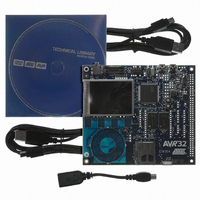
KIT DEV/EVAL FOR AVR32 AT32UC3A
Manufacturer
Atmel
Series
AVR®32r
Type
MCUr
Datasheets
1.ATAVRONE-PROBECBL.pdf
(16 pages)
2.ATEVK1104.pdf
(826 pages)
3.ATEVK1104.pdf
(90 pages)
4.ATEVK1104.pdf
(6 pages)
5.ATEVK1104.pdf
(12 pages)
Specifications of ATEVK1104
Contents
Evaluation Board, Software and Documentation
Processor To Be Evaluated
AT32UC3A3
Data Bus Width
32 bit
Interface Type
USB, SPI, USART
Silicon Manufacturer
Atmel
Core Architecture
AVR
Core Sub-architecture
AVR UC3
Silicon Core Number
AT32UC3A3256
Silicon Family Name
AVR
Kit Contents
Board CD Docs
Rohs Compliant
Yes
For Use With/related Products
AT32UC3A3
Lead Free Status / RoHS Status
Lead free / RoHS Compliant
Available stocks
Company
Part Number
Manufacturer
Quantity
Price
Company:

Part Number:
ATEVK1104
Manufacturer:
Atmel
Quantity:
135


36.8
36.8.1
36.8.2
36.8.3
36.8.4
32058J–AVR32–04/11
Public JTAG instructions
IDCODE
SAMPLE_PRELOAD
EXTEST
INTEST
For description of what memory locations remain accessible, please refer to the SAB address
map.
Full access to these instructions is re-enabled when the security fuse is erased by the
CHIP_ERASE JTAG instruction.
Note that the security bit will read as programmed and block these instructions also if the Flash
Controller is statically reset.
Other security mechanisms can also restrict these functions. If such mechanisms are present
they are listed in the SAB address map section.
This instruction selects the 32 bit ID register as Data Register. The ID register consists of a ver-
sion number, a device number and the manufacturer code chosen by JEDEC. This is the default
instruction after power-up.
The active states are:
JTAG instruction for taking a snap-shot of the input/output pins without affecting the system
operation, and pre-loading the scan chain without updating the DR-latch. The Boundary-Scan
Chain is selected as Data Register.
The active states are:
JTAG instruction for selecting the Boundary-Scan Chain as Data Register for testing circuitry
external to the AVR32 package. The contents of the latched outputs of the Boundary-Scan chain
is driven out as soon as the JTAG IR-register is loaded with the EXTEST instruction.
The active states are:
This instruction selects the Boundary-Scan Chain as Data Register for testing internal logic in
the device. The logic inputs are determined by the Boundary-Scan Chain, and the logic outputs
are captured by the Boundary-Scan chain. The device output pins are driven from the Boundary-
Scan Chain.
The active states are:
• Capture-DR: The static IDCODE value is latched into the shift register.
• Shift-DR: The IDCODE scan chain is shifted by the TCK input.
• Capture-DR: Data on the external pins are sampled into the Boundary-Scan Chain.
• Shift-DR: The Boundary-Scan Chain is shifted by the TCK input.
• Capture-DR: Data on the external pins is sampled into the Boundary-Scan Chain.
• Shift-DR: The Internal Scan Chain is shifted by the TCK input.
• Update-DR: Data from the scan chain is applied to output pins.
• Capture-DR: Data from the internal logic is sampled into the Boundary-Scan Chain.
AT32UC3A
749
Related parts for ATEVK1104
Image
Part Number
Description
Manufacturer
Datasheet
Request
R

Part Number:
Description:
DEV KIT FOR AVR/AVR32
Manufacturer:
Atmel
Datasheet:

Part Number:
Description:
INTERVAL AND WIPE/WASH WIPER CONTROL IC WITH DELAY
Manufacturer:
ATMEL Corporation
Datasheet:
Part Number:
Description:
Low-Voltage Voice-Switched IC for Hands-Free Operation
Manufacturer:
ATMEL Corporation
Datasheet:
Part Number:
Description:
MONOLITHIC INTEGRATED FEATUREPHONE CIRCUIT
Manufacturer:
ATMEL Corporation
Datasheet:
Part Number:
Description:
AM-FM Receiver IC U4255BM-M
Manufacturer:
ATMEL Corporation
Datasheet:
Part Number:
Description:
Monolithic Integrated Feature Phone Circuit
Manufacturer:
ATMEL Corporation
Datasheet:
Part Number:
Description:
Multistandard Video-IF and Quasi Parallel Sound Processing
Manufacturer:
ATMEL Corporation
Datasheet:
Part Number:
Description:
High-performance EE PLD
Manufacturer:
ATMEL Corporation
Datasheet:
Part Number:
Description:
8-bit Flash Microcontroller
Manufacturer:
ATMEL Corporation
Datasheet:
Part Number:
Description:
2-Wire Serial EEPROM
Manufacturer:
ATMEL Corporation
Datasheet: