ATEVK1104 Atmel, ATEVK1104 Datasheet - Page 750
ATEVK1104
Manufacturer Part Number
ATEVK1104
Description
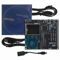
KIT DEV/EVAL FOR AVR32 AT32UC3A
Manufacturer
Atmel
Series
AVR®32r
Type
MCUr
Datasheets
1.ATAVRONE-PROBECBL.pdf
(16 pages)
2.ATEVK1104.pdf
(826 pages)
3.ATEVK1104.pdf
(90 pages)
4.ATEVK1104.pdf
(6 pages)
5.ATEVK1104.pdf
(12 pages)
Specifications of ATEVK1104
Contents
Evaluation Board, Software and Documentation
Processor To Be Evaluated
AT32UC3A3
Data Bus Width
32 bit
Interface Type
USB, SPI, USART
Silicon Manufacturer
Atmel
Core Architecture
AVR
Core Sub-architecture
AVR UC3
Silicon Core Number
AT32UC3A3256
Silicon Family Name
AVR
Kit Contents
Board CD Docs
Rohs Compliant
Yes
For Use With/related Products
AT32UC3A3
Lead Free Status / RoHS Status
Lead free / RoHS Compliant
Available stocks
Company
Part Number
Manufacturer
Quantity
Price
Company:

Part Number:
ATEVK1104
Manufacturer:
Atmel
Quantity:
135


36.8.5
36.8.6
36.9
36.9.1
32058J–AVR32–04/11
Private JTAG Instructions
CLAMP
BYPASS
Notation
This instruction selects the Bypass register as Data Register. The device output pins are driven
from the Boundary-Scan Chain.
The active states are:
The active states are:
The AVR32 defines a number of private JTAG instructions. Each instruction is briefly described
in text, with details following in table form.
Table 36-4 on page 751
corresponds to one bit, and eight bits are grouped together for readability. The rightmost bit is
always shifted first, and the leftmost bit shifted last. The symbols used are shown in
Table 36-3.
In many cases, it is not required to shift all bits through the data register. Bit patterns are shown
using the full width of the shift register, but the suggested or required bits are emphasized using
JTAG instruction selecting the 1-bit Bypass Register for Data Register.
• Shift-DR: The Internal Scan Chain is shifted by the TCK input.
• Update-DR: Data from the scan chain is applied to internal logic inputs.
• Capture-DR: Loads a logic ‘0’ into the Bypass Register.
• Shift-DR: Data is scanned from TDI to TDO through the Bypass register.
• Capture-DR: Loads a logic ‘0’ into the Bypass Register.
• Shift-DR: Data is scanned from TDI to TDO through the Bypass register.
Symbol
0
1
a
b
d
e
p
s
x
r
Description
Constant low value - always reads as zero.
Constant high value - always reads as one.
An address bit - always scanned with the least significant bit first
A busy bit. Reads as one if the SAB was busy, or zero if it was not. See
details on how the busy reporting works.
A data bit - always scanned with the least significant bit first.
An error bit. Reads as one if an error occurred, or zero if not. See
on how the error reporting works.
The chip protected bit. Some devices may be set in a protected state where access to chip
internals are severely restricted. See the documentation for the specific device for details.
On devices without this possibility, this bit always reads as zero.
A direction bit. Set to one to request a read, set to zero to request a write.
A size bit. The size encoding is described where used.
A don’t care bit. Any value can be shifted in, and output data should be ignored.
Symbol description
shows bit patterns to be shifted in a format like " peb01 ". Each character
Section 36.6.4.2
AT32UC3A
Section 36.6.4.1
Table
for details
36-3.
for
750
Related parts for ATEVK1104
Image
Part Number
Description
Manufacturer
Datasheet
Request
R

Part Number:
Description:
DEV KIT FOR AVR/AVR32
Manufacturer:
Atmel
Datasheet:

Part Number:
Description:
INTERVAL AND WIPE/WASH WIPER CONTROL IC WITH DELAY
Manufacturer:
ATMEL Corporation
Datasheet:
Part Number:
Description:
Low-Voltage Voice-Switched IC for Hands-Free Operation
Manufacturer:
ATMEL Corporation
Datasheet:
Part Number:
Description:
MONOLITHIC INTEGRATED FEATUREPHONE CIRCUIT
Manufacturer:
ATMEL Corporation
Datasheet:
Part Number:
Description:
AM-FM Receiver IC U4255BM-M
Manufacturer:
ATMEL Corporation
Datasheet:
Part Number:
Description:
Monolithic Integrated Feature Phone Circuit
Manufacturer:
ATMEL Corporation
Datasheet:
Part Number:
Description:
Multistandard Video-IF and Quasi Parallel Sound Processing
Manufacturer:
ATMEL Corporation
Datasheet:
Part Number:
Description:
High-performance EE PLD
Manufacturer:
ATMEL Corporation
Datasheet:
Part Number:
Description:
8-bit Flash Microcontroller
Manufacturer:
ATMEL Corporation
Datasheet:
Part Number:
Description:
2-Wire Serial EEPROM
Manufacturer:
ATMEL Corporation
Datasheet: