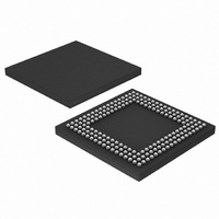
LPC2458FET180,551 NXP Semiconductors, LPC2458FET180,551 Datasheet - Page 667

LPC2458FET180,551
Manufacturer Part Number
LPC2458FET180,551
Description
IC ARM7 MCU FLASH 512K 180TFBGA
Manufacturer
NXP Semiconductors
Series
LPC2400r
Specifications of LPC2458FET180,551
Core Processor
ARM7
Core Size
16/32-Bit
Speed
72MHz
Connectivity
CAN, EBI/EMI, Ethernet, I²C, Microwire, MMC, SPI, SSI, SSP, UART/USART, USB OTG
Peripherals
Brown-out Detect/Reset, DMA, I²S, POR, PWM, WDT
Number Of I /o
136
Program Memory Size
512KB (512K x 8)
Program Memory Type
FLASH
Ram Size
98K x 8
Voltage - Supply (vcc/vdd)
3 V ~ 3.6 V
Data Converters
A/D 8x10b; D/A 1x10b
Oscillator Type
Internal
Operating Temperature
-40°C ~ 85°C
Package / Case
180-TFBGA
Processor Series
LPC24
Core
ARM7TDMI-S
Data Bus Width
32 bit
Data Ram Size
98 KB
Interface Type
CAN, Ethernet, I2C, I2S, IrDA, SPI, SSP, UART, USB
Maximum Clock Frequency
72 MHz
Number Of Programmable I/os
136
Number Of Timers
4
Operating Supply Voltage
3.3 V
Maximum Operating Temperature
+ 85 C
Mounting Style
SMD/SMT
3rd Party Development Tools
MDK-ARM, RL-ARM, ULINK2, SAB-TFBGA180
Minimum Operating Temperature
- 40 C
On-chip Adc
10 bit, 8 Channel
On-chip Dac
10 bit, 1 Channel
Package
180TFBGA
Device Core
ARM7TDMI-S
Family Name
LPC2000
Maximum Speed
72 MHz
For Use With
622-1023 - BOARD SCKT ADAPTER FOR TFBGA180622-1005 - USB IN-CIRCUIT PROG ARM7 LPC2K
Lead Free Status / RoHS Status
Lead free / RoHS Compliant
Eeprom Size
-
Lead Free Status / Rohs Status
Details
Other names
568-4258
935282454551
LPC2458FET180-S
935282454551
LPC2458FET180-S
Available stocks
Company
Part Number
Manufacturer
Quantity
Price
Company:
Part Number:
LPC2458FET180,551
Manufacturer:
MICROCHIP
Quantity:
1 103
Company:
Part Number:
LPC2458FET180,551
Manufacturer:
NXP Semiconductors
Quantity:
10 000
- Current page: 667 of 792
- Download datasheet (5Mb)
1. Basic configuration
2. Features
3. Description
4. Pin description
UM10237_4
User manual
The ADC is configured using the following registers:
Basic clocking for the A/D converters is provided by the APB clock (PCLK). A
programmable divider is included in each converter, to scale this clock to the 4.5 MHz
(max) clock needed by the successive approximation process. A fully accurate conversion
requires 11 of these clocks.
Table 28–591
1. Power: In the PCONP register
2. Clock: In the PCLK_SEL0 register
3. Pins: Select ADC pins and pin modes in registers PINSELn and PINMODEn (see
4. Interrupts: To enable interrupts in the ADC, see
•
•
•
•
•
•
•
•
UM10237
Chapter 28: LPC24XX Analog-to Digital Converter (ADC)
Rev. 04 — 26 August 2009
Remark: On reset, the ADC is disabled. To enable the ADC, first set the PCADC bit,
and then enable the ADC in the AD0CR register (bit PDN)
the ADC, first clear the PDN bit, and then clear the PCADC bit.
clock for the ADC, see
Section
in the VIC using the VICIntEnable register
10 bit successive approximation analog to digital converter.
Input multiplexing among 8 pins.
Power-down mode.
Measurement range 0 to 3 V.
10 bit conversion time ≥ 2.44 μs.
Burst conversion mode for single or multiple inputs.
Optional conversion on transition on input pin or Timer Match signal.
Individual result registers for each A/D channel to reduce interrupt overhead.
9–5).
gives a brief summary of each of ADC related pins.
Rev. 04 — 26 August 2009
Table 28–593
(Table
(Table
bits CLKDIV.
4–63), set bits PCADC.
4–56), select PCLK_ADC. To scale the
(Section
Table
7–3.4).
28–596. Interrupts are enabled
Table
28–593. To disable
© NXP B.V. 2009. All rights reserved.
User manual
667 of 792
Related parts for LPC2458FET180,551
Image
Part Number
Description
Manufacturer
Datasheet
Request
R

Part Number:
Description:
NXP Semiconductors designed the LPC2458 microcontroller around a 16-bit/32-bitARM7TDMI-S CPU core with real-time debug interfaces that include both JTAG andembedded trace
Manufacturer:
NXP Semiconductors
Datasheet:
Part Number:
Description:
NXP Semiconductors designed the LPC2420/2460 microcontroller around a 16-bit/32-bitARM7TDMI-S CPU core with real-time debug interfaces that include both JTAG andembedded trace
Manufacturer:
NXP Semiconductors
Datasheet:
Part Number:
Description:
NXP Semiconductors designed the LPC2468 microcontroller around a 16-bit/32-bitARM7TDMI-S CPU core with real-time debug interfaces that include both JTAG andembedded trace
Manufacturer:
NXP Semiconductors
Datasheet:
Part Number:
Description:
NXP Semiconductors designed the LPC2470 microcontroller, powered by theARM7TDMI-S core, to be a highly integrated microcontroller for a wide range ofapplications that require advanced communications and high quality graphic displays
Manufacturer:
NXP Semiconductors
Datasheet:
Part Number:
Description:
NXP Semiconductors designed the LPC2478 microcontroller, powered by theARM7TDMI-S core, to be a highly integrated microcontroller for a wide range ofapplications that require advanced communications and high quality graphic displays
Manufacturer:
NXP Semiconductors
Datasheet:
Part Number:
Description:
The Philips Semiconductors XA (eXtended Architecture) family of 16-bit single-chip microcontrollers is powerful enough to easily handle the requirements of high performance embedded applications, yet inexpensive enough to compete in the market for hi
Manufacturer:
NXP Semiconductors
Datasheet:
Part Number:
Description:
The XA-S3 device is a member of Philips Semiconductors? XA(eXtended Architecture) family of high performance 16-bitsingle-chip microcontrollers
Manufacturer:
NXP Semiconductors
Datasheet:

Part Number:
Description:
The NXP BlueStreak LH75401/LH75411 family consists of two low-cost 16/32-bit System-on-Chip (SoC) devices
Manufacturer:
NXP Semiconductors
Datasheet:

Part Number:
Description:
The NXP LPC3130/3131 combine an 180 MHz ARM926EJ-S CPU core, high-speed USB2
Manufacturer:
NXP Semiconductors
Datasheet:

Part Number:
Description:
The NXP LPC3141 combine a 270 MHz ARM926EJ-S CPU core, High-speed USB 2
Manufacturer:
NXP Semiconductors

Part Number:
Description:
The NXP LPC3143 combine a 270 MHz ARM926EJ-S CPU core, High-speed USB 2
Manufacturer:
NXP Semiconductors

Part Number:
Description:
The NXP LPC3152 combines an 180 MHz ARM926EJ-S CPU core, High-speed USB 2
Manufacturer:
NXP Semiconductors

Part Number:
Description:
The NXP LPC3154 combines an 180 MHz ARM926EJ-S CPU core, High-speed USB 2
Manufacturer:
NXP Semiconductors

Part Number:
Description:
Standard level N-channel enhancement mode Field-Effect Transistor (FET) in a plastic package using NXP High-Performance Automotive (HPA) TrenchMOS technology
Manufacturer:
NXP Semiconductors
Datasheet:


