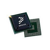
MPC5125YVN400 Freescale Semiconductor, MPC5125YVN400 Datasheet - Page 109

MPC5125YVN400
Manufacturer Part Number
MPC5125YVN400
Description
IC MCU 32BIT E300 324TEPBGA
Manufacturer
Freescale Semiconductor
Series
MPC51xxr
Datasheets
1.MPC5125YVN400.pdf
(92 pages)
2.MPC5125YVN400.pdf
(8 pages)
3.MPC5125YVN400.pdf
(2 pages)
4.MPC5125YVN400.pdf
(1064 pages)
Specifications of MPC5125YVN400
Core Processor
e300
Core Size
32-Bit
Speed
400MHz
Connectivity
CAN, EBI/EMI, Ethernet, I²C, USB OTG
Peripherals
DMA, WDT
Number Of I /o
64
Program Memory Type
ROMless
Ram Size
32K x 8
Voltage - Supply (vcc/vdd)
1.33 V ~ 1.47 V
Oscillator Type
External
Operating Temperature
-40°C ~ 125°C
Package / Case
324-PBGA
Processor Series
MPC51xx
Core
e300
Data Bus Width
32 bit
Development Tools By Supplier
TWR-MPC5125-KIT, TWR-SER, TWR-ELEV, TOWER
Maximum Clock Frequency
400 MHz
Operating Supply Voltage
1.4 V
Maximum Operating Temperature
+ 125 C
Mounting Style
SMD/SMT
Data Ram Size
32 KB
I/o Voltage
3.3 V
Interface Type
CAN, I2C
Minimum Operating Temperature
- 40 C
Program Memory Size
32 bit
Cpu Speed
400MHz
Embedded Interface Type
CAN, I2C, SPI, UART, USB
Digital Ic Case Style
TEPBGA
No. Of Pins
324
Rohs Compliant
Yes
Cpu Family
MPC5xx
Device Core Size
32b
Frequency (max)
400MHz
Total Internal Ram Size
32KB
Instruction Set Architecture
RISC
Operating Temp Range
-40C to 85C
Operating Temperature Classification
Industrial
Mounting
Surface Mount
Pin Count
324
Lead Free Status / RoHS Status
Lead free / RoHS Compliant
Eeprom Size
-
Program Memory Size
-
Data Converters
-
Lead Free Status / Rohs Status
Lead free / RoHS Compliant
Available stocks
Company
Part Number
Manufacturer
Quantity
Price
Company:
Part Number:
MPC5125YVN400
Manufacturer:
Freescale Semiconductor
Quantity:
135
Company:
Part Number:
MPC5125YVN400
Manufacturer:
LTC
Quantity:
29
Company:
Part Number:
MPC5125YVN400
Manufacturer:
Freescale Semiconductor
Quantity:
10 000
- MPC5125YVN400 PDF datasheet
- MPC5125YVN400 PDF datasheet #2
- MPC5125YVN400 PDF datasheet #3
- MPC5125YVN400 PDF datasheet #4
- Current page: 109 of 1064
- Download datasheet (6Mb)
5.3.1.2
The System Clock Control Register 1 shown in
ratio.
1
Freescale Semiconductor
Address: Base + 0x04
Bit is reserved, and must not be written or cleared. Value must remain 1.
Reset
Reset
CMPF
SPMF
Field
W
W
R CFG_
R FIFO
C_EN
EN
16
1
0
0
System Clock Control Register 1 (SCCR1)
System PLL Multiplication Factor. See
Core PLL Configuration. See
LPC_
EN
17
1
0
0
1
NFC_
FEC1
_EN
EN
18
1
0
2
1
Figure 5-7. System Clock Control Register 1 (SCCR1)
All the clocks from CLOCK block are bypassed with PLL reference clock.
1
CPMF
19
0
0
0
3
SPMF
001
010
011
1
00x
MPC5125 Microcontroller Reference Manual, Rev. 2
0000
0001
0010
0011
0100
0101
0110
0111
PSC0
_EN
20
4
0
0
1
Table 5-6. SPMR field descriptions
Core PLL BYPASS / OFF
DDR_
PSC1
Section 5.2.8.2, “e300 Core PLL Programming Model,” on page
_EN
EN
21
0
1
5
f
PLL BYPASS
cpll
f
spll
PSC2
FEC2
_EN
_EN
1.0: 1
1.5: 1
36:1
: f
22
0
0
Section 5.2.8.1, “System PLL Programming Model,” on page
Figure 5-7
6
68:1
12:1
16:1
20:1
24:1
28:1
32:1
: f
csb_clk
ref_clk
PSC3
_EN
23
0
0
0
7
1
Description
PSC4
_EN
controls device units with a configurable clock
24
8
0
0
0
PSC5
SPMF
CPMF
_EN
1000
1001
1010
1011
1100
1101
1110
1111
100
101
110
111
25
9
0
0
0
PSC6
_EN
10
26
0
0
0
PSC7
_EN
11
27
0
0
0
f
f
spll
cpll
Clocks and Low-Power Modes
36:1
40:1
44:1
48:1
52:1
56:1
60:1
64:1
PSC8
: f
2.0: 1
2.5: 1
3.0: 1
3.5: 1
: f
_EN
12
28
0
0
0
ref_clk
csb_clk
Access: User read/write
PSC9
_EN
13
29
0
0
0
5-6.
14
30
0
0
0
0
5-5.
15
31
0
0
0
0
5-9
Related parts for MPC5125YVN400
Image
Part Number
Description
Manufacturer
Datasheet
Request
R
Part Number:
Description:
Mpc5125 Microcontroller Data Sheet
Manufacturer:
Freescale Semiconductor, Inc
Datasheet:

Part Number:
Description:
MPC5125 Microcontroller Data Sheet
Manufacturer:
FREESCALE [Freescale Semiconductor, Inc]
Datasheet:
Part Number:
Description:
Manufacturer:
Freescale Semiconductor, Inc
Datasheet:
Part Number:
Description:
Manufacturer:
Freescale Semiconductor, Inc
Datasheet:
Part Number:
Description:
Manufacturer:
Freescale Semiconductor, Inc
Datasheet:
Part Number:
Description:
Manufacturer:
Freescale Semiconductor, Inc
Datasheet:
Part Number:
Description:
Manufacturer:
Freescale Semiconductor, Inc
Datasheet:
Part Number:
Description:
Manufacturer:
Freescale Semiconductor, Inc
Datasheet:
Part Number:
Description:
Manufacturer:
Freescale Semiconductor, Inc
Datasheet:
Part Number:
Description:
Manufacturer:
Freescale Semiconductor, Inc
Datasheet:
Part Number:
Description:
Manufacturer:
Freescale Semiconductor, Inc
Datasheet:
Part Number:
Description:
Manufacturer:
Freescale Semiconductor, Inc
Datasheet:
Part Number:
Description:
Manufacturer:
Freescale Semiconductor, Inc
Datasheet:
Part Number:
Description:
Manufacturer:
Freescale Semiconductor, Inc
Datasheet:
Part Number:
Description:
Manufacturer:
Freescale Semiconductor, Inc
Datasheet:


