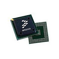
MPC5125YVN400 Freescale Semiconductor, MPC5125YVN400 Datasheet - Page 633

MPC5125YVN400
Manufacturer Part Number
MPC5125YVN400
Description
IC MCU 32BIT E300 324TEPBGA
Manufacturer
Freescale Semiconductor
Series
MPC51xxr
Datasheets
1.MPC5125YVN400.pdf
(92 pages)
2.MPC5125YVN400.pdf
(8 pages)
3.MPC5125YVN400.pdf
(2 pages)
4.MPC5125YVN400.pdf
(1064 pages)
Specifications of MPC5125YVN400
Core Processor
e300
Core Size
32-Bit
Speed
400MHz
Connectivity
CAN, EBI/EMI, Ethernet, I²C, USB OTG
Peripherals
DMA, WDT
Number Of I /o
64
Program Memory Type
ROMless
Ram Size
32K x 8
Voltage - Supply (vcc/vdd)
1.33 V ~ 1.47 V
Oscillator Type
External
Operating Temperature
-40°C ~ 125°C
Package / Case
324-PBGA
Processor Series
MPC51xx
Core
e300
Data Bus Width
32 bit
Development Tools By Supplier
TWR-MPC5125-KIT, TWR-SER, TWR-ELEV, TOWER
Maximum Clock Frequency
400 MHz
Operating Supply Voltage
1.4 V
Maximum Operating Temperature
+ 125 C
Mounting Style
SMD/SMT
Data Ram Size
32 KB
I/o Voltage
3.3 V
Interface Type
CAN, I2C
Minimum Operating Temperature
- 40 C
Program Memory Size
32 bit
Cpu Speed
400MHz
Embedded Interface Type
CAN, I2C, SPI, UART, USB
Digital Ic Case Style
TEPBGA
No. Of Pins
324
Rohs Compliant
Yes
Cpu Family
MPC5xx
Device Core Size
32b
Frequency (max)
400MHz
Total Internal Ram Size
32KB
Instruction Set Architecture
RISC
Operating Temp Range
-40C to 85C
Operating Temperature Classification
Industrial
Mounting
Surface Mount
Pin Count
324
Lead Free Status / RoHS Status
Lead free / RoHS Compliant
Eeprom Size
-
Program Memory Size
-
Data Converters
-
Lead Free Status / Rohs Status
Lead free / RoHS Compliant
Available stocks
Company
Part Number
Manufacturer
Quantity
Price
Company:
Part Number:
MPC5125YVN400
Manufacturer:
Freescale Semiconductor
Quantity:
135
Company:
Part Number:
MPC5125YVN400
Manufacturer:
LTC
Quantity:
29
Company:
Part Number:
MPC5125YVN400
Manufacturer:
Freescale Semiconductor
Quantity:
10 000
- MPC5125YVN400 PDF datasheet
- MPC5125YVN400 PDF datasheet #2
- MPC5125YVN400 PDF datasheet #3
- MPC5125YVN400 PDF datasheet #4
- Current page: 633 of 1064
- Download datasheet (6Mb)
23.5
Figure 23-2
bits, and is separated into 4 buffers. Each buffer has a non-contiguous physical address. For example,
buffer0’s physical address is (0x0000 + 0x0020 × i) ~ (0x0007 + 0x0020 × i).
When the CPU is writing or reading a buffer in no- boot mode, the CPU address is continuous, because an
address transition is provided inside the NFC:
sram_physical_addr[13:3] = {cpu_addr[11:3],cpu_addr[13:12]}.
So in non-boot mode, buffer0’s address range is 0x0000–0x08FF, buffer1 is 0x1000–0x18FF, buffer2 is
0x2000–0x28FF, buffer3 is 0x3000–0x38FF.
See
Freescale Semiconductor
Figure 23-25
NFC Buffer Memory Space
shows the organization of the buffer memory space in the NFC. The memory size is 1152 × 64
NFC_IO[15:0]
NFC_R/B0
NFC_R/B1
NFC_R/B2
NFC_R/B3
NFC_ALE
NFC_CE0
NFC_CE1
NFC_CE2
NFC_CE3
NFC_CLE
NFC_WE
NFC_RE
for the different operations between boot mode and non-boot mode.
Name
MPC5125 Microcontroller Reference Manual, Rev. 2
Flash Address Latch Enable
Flash #0 Chip Enable
Flash #1 Chip Enable
Flash #2 Chip Enable
Flash #3 Chip Enable
Flash Command Latch Enable
Flash #0 Ready/Busy
Flash #1 Ready/Busy
Flash #2 Ready/Busy
Flash #3 Ready/Busy
Flash Read Enable
Flash Write Enable
Flash data bus
Table 23-1. NFC Signal Properties
Function
I/O
I/O
NAND Flash Controller (NFC)
O
O
O
O
O
O
O
O
I
I
I
I
Reset
—
—
—
—
—
0
1
1
1
1
1
1
0
23-3
Related parts for MPC5125YVN400
Image
Part Number
Description
Manufacturer
Datasheet
Request
R
Part Number:
Description:
Mpc5125 Microcontroller Data Sheet
Manufacturer:
Freescale Semiconductor, Inc
Datasheet:

Part Number:
Description:
MPC5125 Microcontroller Data Sheet
Manufacturer:
FREESCALE [Freescale Semiconductor, Inc]
Datasheet:
Part Number:
Description:
Manufacturer:
Freescale Semiconductor, Inc
Datasheet:
Part Number:
Description:
Manufacturer:
Freescale Semiconductor, Inc
Datasheet:
Part Number:
Description:
Manufacturer:
Freescale Semiconductor, Inc
Datasheet:
Part Number:
Description:
Manufacturer:
Freescale Semiconductor, Inc
Datasheet:
Part Number:
Description:
Manufacturer:
Freescale Semiconductor, Inc
Datasheet:
Part Number:
Description:
Manufacturer:
Freescale Semiconductor, Inc
Datasheet:
Part Number:
Description:
Manufacturer:
Freescale Semiconductor, Inc
Datasheet:
Part Number:
Description:
Manufacturer:
Freescale Semiconductor, Inc
Datasheet:
Part Number:
Description:
Manufacturer:
Freescale Semiconductor, Inc
Datasheet:
Part Number:
Description:
Manufacturer:
Freescale Semiconductor, Inc
Datasheet:
Part Number:
Description:
Manufacturer:
Freescale Semiconductor, Inc
Datasheet:
Part Number:
Description:
Manufacturer:
Freescale Semiconductor, Inc
Datasheet:
Part Number:
Description:
Manufacturer:
Freescale Semiconductor, Inc
Datasheet:


