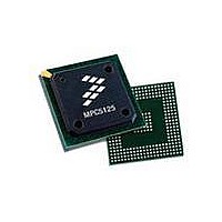
MPC5125YVN400 Freescale Semiconductor, MPC5125YVN400 Datasheet - Page 406

MPC5125YVN400
Manufacturer Part Number
MPC5125YVN400
Description
IC MCU 32BIT E300 324TEPBGA
Manufacturer
Freescale Semiconductor
Series
MPC51xxr
Datasheets
1.MPC5125YVN400.pdf
(92 pages)
2.MPC5125YVN400.pdf
(8 pages)
3.MPC5125YVN400.pdf
(2 pages)
4.MPC5125YVN400.pdf
(1064 pages)
Specifications of MPC5125YVN400
Core Processor
e300
Core Size
32-Bit
Speed
400MHz
Connectivity
CAN, EBI/EMI, Ethernet, I²C, USB OTG
Peripherals
DMA, WDT
Number Of I /o
64
Program Memory Type
ROMless
Ram Size
32K x 8
Voltage - Supply (vcc/vdd)
1.33 V ~ 1.47 V
Oscillator Type
External
Operating Temperature
-40°C ~ 125°C
Package / Case
324-PBGA
Processor Series
MPC51xx
Core
e300
Data Bus Width
32 bit
Development Tools By Supplier
TWR-MPC5125-KIT, TWR-SER, TWR-ELEV, TOWER
Maximum Clock Frequency
400 MHz
Operating Supply Voltage
1.4 V
Maximum Operating Temperature
+ 125 C
Mounting Style
SMD/SMT
Data Ram Size
32 KB
I/o Voltage
3.3 V
Interface Type
CAN, I2C
Minimum Operating Temperature
- 40 C
Program Memory Size
32 bit
Cpu Speed
400MHz
Embedded Interface Type
CAN, I2C, SPI, UART, USB
Digital Ic Case Style
TEPBGA
No. Of Pins
324
Rohs Compliant
Yes
Cpu Family
MPC5xx
Device Core Size
32b
Frequency (max)
400MHz
Total Internal Ram Size
32KB
Instruction Set Architecture
RISC
Operating Temp Range
-40C to 85C
Operating Temperature Classification
Industrial
Mounting
Surface Mount
Pin Count
324
Lead Free Status / RoHS Status
Lead free / RoHS Compliant
Eeprom Size
-
Program Memory Size
-
Data Converters
-
Lead Free Status / Rohs Status
Lead free / RoHS Compliant
Available stocks
Company
Part Number
Manufacturer
Quantity
Price
Company:
Part Number:
MPC5125YVN400
Manufacturer:
Freescale Semiconductor
Quantity:
135
Company:
Part Number:
MPC5125YVN400
Manufacturer:
LTC
Quantity:
29
Company:
Part Number:
MPC5125YVN400
Manufacturer:
Freescale Semiconductor
Quantity:
10 000
- MPC5125YVN400 PDF datasheet
- MPC5125YVN400 PDF datasheet #2
- MPC5125YVN400 PDF datasheet #3
- MPC5125YVN400 PDF datasheet #4
- Current page: 406 of 1064
- Download datasheet (6Mb)
Fast Ethernet Controller (FEC)
When the transmitter is paused due to receiver/descriptor controller pause frame detection, transmit flow
control pause (TFC_PAUSE) may continue to be asserted and cause the transmission of a single pause
frame. In this case, the GRA interrupt is not asserted.
14.6.5
The minimum inter-packet gap time for back-to-back transmission is 96 bit times. After completing a
transmission or after the backoff algorithm completes, the transmitter waits for carrier sense to be negated
before starting its 96 bit time IPG counter. Frame transmission may begin 96 bit times after carrier sense
is negated if it stays negated for at least 60 bit times. If carrier sense asserts during the last 36 bit times, it
is ignored and a collision occurs.
The receiver receives back-to-back frames with a minimum spacing of at least 28 bit times. If an
inter-packet gap between receive frames is less than 28 bit counts, the following frame may be discarded
by the receiver.
14.6.6
If a collision occurs during frame transmission, the Ethernet controller continues the transmission for at
least 32 bit times, transmitting a jam pattern consisting of 32 ones. If the collision occurs during the
preamble sequence, the jam pattern is sent after the end of the preamble sequence.
If a collision occurs within 64 byte times, the retry process is initiated. The transmitter waits a random
number of slot times. A slot time is 512 bit times. If a collision occurs after 64 byte times, no
retransmission is performed and the end-of-frame buffer is closed with an LC error indication.
14.6.7
Internal and external loopback are supported by the Ethernet controller. In loopback mode, both of the
FIFOs are used and the FEC actually operates in a full-duplex fashion. Internal and external loopback are
configured using combinations of the LOOP and DRT bits in the ETH_R_CNTRL register and the FDEN
bit in the ETH_X_CNTRL register.
For internal and external loopback, set FDEN equal to 1.
For internal loopback, set LOOP equal to 1 and DRT equal to 0. TX_EN and TX_ER do not assert during
internal loopback. During internal loopback, the transmit/receive data rate is higher than in normal
operation because the internal system clock is used by the transmit and receive blocks instead of the clocks
from the external transceiver. This causes an increase in the required system bus bandwidth for transmit
and receive data being direct memory addressed to/from external memory. It may be necessary to pace the
frames on the transmit side and/or limit the size of the frames to prevent transmit FIFO underrun and
receive FIFO overflow.
For external loopback, set LOOP equal to 0 and DRT equal 0, and then configure the external transceiver
for loopback.
14-50
Inter-Packet Gap Time
Collision Handling
MII Internal and External Loopback
MPC5125 Microcontroller Reference Manual, Rev. 2
Freescale Semiconductor
Related parts for MPC5125YVN400
Image
Part Number
Description
Manufacturer
Datasheet
Request
R
Part Number:
Description:
Mpc5125 Microcontroller Data Sheet
Manufacturer:
Freescale Semiconductor, Inc
Datasheet:

Part Number:
Description:
MPC5125 Microcontroller Data Sheet
Manufacturer:
FREESCALE [Freescale Semiconductor, Inc]
Datasheet:
Part Number:
Description:
Manufacturer:
Freescale Semiconductor, Inc
Datasheet:
Part Number:
Description:
Manufacturer:
Freescale Semiconductor, Inc
Datasheet:
Part Number:
Description:
Manufacturer:
Freescale Semiconductor, Inc
Datasheet:
Part Number:
Description:
Manufacturer:
Freescale Semiconductor, Inc
Datasheet:
Part Number:
Description:
Manufacturer:
Freescale Semiconductor, Inc
Datasheet:
Part Number:
Description:
Manufacturer:
Freescale Semiconductor, Inc
Datasheet:
Part Number:
Description:
Manufacturer:
Freescale Semiconductor, Inc
Datasheet:
Part Number:
Description:
Manufacturer:
Freescale Semiconductor, Inc
Datasheet:
Part Number:
Description:
Manufacturer:
Freescale Semiconductor, Inc
Datasheet:
Part Number:
Description:
Manufacturer:
Freescale Semiconductor, Inc
Datasheet:
Part Number:
Description:
Manufacturer:
Freescale Semiconductor, Inc
Datasheet:
Part Number:
Description:
Manufacturer:
Freescale Semiconductor, Inc
Datasheet:
Part Number:
Description:
Manufacturer:
Freescale Semiconductor, Inc
Datasheet:


