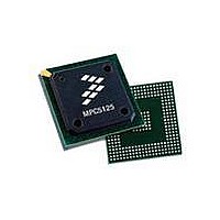
MPC5125YVN400 Freescale Semiconductor, MPC5125YVN400 Datasheet - Page 639

MPC5125YVN400
Manufacturer Part Number
MPC5125YVN400
Description
IC MCU 32BIT E300 324TEPBGA
Manufacturer
Freescale Semiconductor
Series
MPC51xxr
Datasheets
1.MPC5125YVN400.pdf
(92 pages)
2.MPC5125YVN400.pdf
(8 pages)
3.MPC5125YVN400.pdf
(2 pages)
4.MPC5125YVN400.pdf
(1064 pages)
Specifications of MPC5125YVN400
Core Processor
e300
Core Size
32-Bit
Speed
400MHz
Connectivity
CAN, EBI/EMI, Ethernet, I²C, USB OTG
Peripherals
DMA, WDT
Number Of I /o
64
Program Memory Type
ROMless
Ram Size
32K x 8
Voltage - Supply (vcc/vdd)
1.33 V ~ 1.47 V
Oscillator Type
External
Operating Temperature
-40°C ~ 125°C
Package / Case
324-PBGA
Processor Series
MPC51xx
Core
e300
Data Bus Width
32 bit
Development Tools By Supplier
TWR-MPC5125-KIT, TWR-SER, TWR-ELEV, TOWER
Maximum Clock Frequency
400 MHz
Operating Supply Voltage
1.4 V
Maximum Operating Temperature
+ 125 C
Mounting Style
SMD/SMT
Data Ram Size
32 KB
I/o Voltage
3.3 V
Interface Type
CAN, I2C
Minimum Operating Temperature
- 40 C
Program Memory Size
32 bit
Cpu Speed
400MHz
Embedded Interface Type
CAN, I2C, SPI, UART, USB
Digital Ic Case Style
TEPBGA
No. Of Pins
324
Rohs Compliant
Yes
Cpu Family
MPC5xx
Device Core Size
32b
Frequency (max)
400MHz
Total Internal Ram Size
32KB
Instruction Set Architecture
RISC
Operating Temp Range
-40C to 85C
Operating Temperature Classification
Industrial
Mounting
Surface Mount
Pin Count
324
Lead Free Status / RoHS Status
Lead free / RoHS Compliant
Eeprom Size
-
Program Memory Size
-
Data Converters
-
Lead Free Status / Rohs Status
Lead free / RoHS Compliant
Available stocks
Company
Part Number
Manufacturer
Quantity
Price
Company:
Part Number:
MPC5125YVN400
Manufacturer:
Freescale Semiconductor
Quantity:
135
Company:
Part Number:
MPC5125YVN400
Manufacturer:
LTC
Quantity:
29
Company:
Part Number:
MPC5125YVN400
Manufacturer:
Freescale Semiconductor
Quantity:
10 000
- MPC5125YVN400 PDF datasheet
- MPC5125YVN400 PDF datasheet #2
- MPC5125YVN400 PDF datasheet #3
- MPC5125YVN400 PDF datasheet #4
- Current page: 639 of 1064
- Download datasheet (6Mb)
23.7.3
Freescale Semiconductor
FLASH_CMD_CODE[15:0]
FLASH_CMD_BYTE1[7:0] First command byte that may be sent to flash device.
Address: Base + 0x3F08
Reset
Reset
W
W
BUFNO[1:0]
R
R
START
BUSY
Field
16
0
0
0
0
Column Address register (COL_ADDR)
17
0
0
0
1
18
0
0
0
2
User defined flash operation sequencer. Each bit stands for a certain action.(See
If the bit is set to 1, the corresponding action will be executed, after writing 1 to START field.
Following are some configuration examples: (other sequences are possible.)
0111_1110_1110_0000 : read data (FLASH_CMD_BYTE1, 5x Address, FLASH_CMD_BYTE2,
R/B, read data).
1111_1111_1101_1000 : write page (DMA,FLASH_CMD_BYTE1, 5x Address, write data,
FLASH_CMD_BYTE2, R/B, FLASH_CMD_BYTE3, read status).
0100_1110_1101_1000 : block erase (FLASH_CMD_BYTE1, 3x Address, FLASH_CMD_BYTE2,
R/B, FLASH_CMD_BYTE3, read status).
0100_1000_0000_0100 : Read ID (FLASH_CMD_BYTE1, 1x Address, read ID).
0100_0000_0100_0000 : Reset (FLASH_CMD_BYTE1, R/B).
0111_1110_0000_0000 : CMD+address (FLASH_CMD_BYTE1, 5x Address).
1111_1111_1100_0000 : write page burst (DMA,FLASH_CMD_BYTE1,5xAddress, write data,
FLASH_CMD_BYTE2,R/B).
Internal buffer number used for this command.
this bit is repeated in the interrupt register.
0 Flash controller is idle. OK to sent next command.
1 Command execution is busy.
Note: The reset value is maintained a short period of time. The NFC issues the reset command
0 No action.
1 Command execution starts.
COL_ADDR2[7:0]
Figure 23-5. Column Address register (COL_ADDR)
19
0
0
0
3
0xFF to NAND flash after system reset. After the command is done, the value of BUSY
changes to 0.
MPC5125 Microcontroller Reference Manual, Rev. 2
Table 23-5. FLASH_CMD2 field descriptions
20
4
0
0
0
21
0
0
0
5
22
0
0
0
6
23
0
0
0
7
24
Description
8
0
0
0
25
9
0
0
0
10
26
0
0
0
COL_ADDR1[7:0]
11
27
0
0
0
NAND Flash Controller (NFC)
12
28
0
0
0
Access: User read/write
13
29
0
0
0
Table
14
30
0
0
0
23-22)
15
31
23-9
0
0
0
Related parts for MPC5125YVN400
Image
Part Number
Description
Manufacturer
Datasheet
Request
R
Part Number:
Description:
Mpc5125 Microcontroller Data Sheet
Manufacturer:
Freescale Semiconductor, Inc
Datasheet:

Part Number:
Description:
MPC5125 Microcontroller Data Sheet
Manufacturer:
FREESCALE [Freescale Semiconductor, Inc]
Datasheet:
Part Number:
Description:
Manufacturer:
Freescale Semiconductor, Inc
Datasheet:
Part Number:
Description:
Manufacturer:
Freescale Semiconductor, Inc
Datasheet:
Part Number:
Description:
Manufacturer:
Freescale Semiconductor, Inc
Datasheet:
Part Number:
Description:
Manufacturer:
Freescale Semiconductor, Inc
Datasheet:
Part Number:
Description:
Manufacturer:
Freescale Semiconductor, Inc
Datasheet:
Part Number:
Description:
Manufacturer:
Freescale Semiconductor, Inc
Datasheet:
Part Number:
Description:
Manufacturer:
Freescale Semiconductor, Inc
Datasheet:
Part Number:
Description:
Manufacturer:
Freescale Semiconductor, Inc
Datasheet:
Part Number:
Description:
Manufacturer:
Freescale Semiconductor, Inc
Datasheet:
Part Number:
Description:
Manufacturer:
Freescale Semiconductor, Inc
Datasheet:
Part Number:
Description:
Manufacturer:
Freescale Semiconductor, Inc
Datasheet:
Part Number:
Description:
Manufacturer:
Freescale Semiconductor, Inc
Datasheet:
Part Number:
Description:
Manufacturer:
Freescale Semiconductor, Inc
Datasheet:


