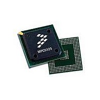
MPC5125YVN400 Freescale Semiconductor, MPC5125YVN400 Datasheet - Page 247

MPC5125YVN400
Manufacturer Part Number
MPC5125YVN400
Description
IC MCU 32BIT E300 324TEPBGA
Manufacturer
Freescale Semiconductor
Series
MPC51xxr
Datasheets
1.MPC5125YVN400.pdf
(92 pages)
2.MPC5125YVN400.pdf
(8 pages)
3.MPC5125YVN400.pdf
(2 pages)
4.MPC5125YVN400.pdf
(1064 pages)
Specifications of MPC5125YVN400
Core Processor
e300
Core Size
32-Bit
Speed
400MHz
Connectivity
CAN, EBI/EMI, Ethernet, I²C, USB OTG
Peripherals
DMA, WDT
Number Of I /o
64
Program Memory Type
ROMless
Ram Size
32K x 8
Voltage - Supply (vcc/vdd)
1.33 V ~ 1.47 V
Oscillator Type
External
Operating Temperature
-40°C ~ 125°C
Package / Case
324-PBGA
Processor Series
MPC51xx
Core
e300
Data Bus Width
32 bit
Development Tools By Supplier
TWR-MPC5125-KIT, TWR-SER, TWR-ELEV, TOWER
Maximum Clock Frequency
400 MHz
Operating Supply Voltage
1.4 V
Maximum Operating Temperature
+ 125 C
Mounting Style
SMD/SMT
Data Ram Size
32 KB
I/o Voltage
3.3 V
Interface Type
CAN, I2C
Minimum Operating Temperature
- 40 C
Program Memory Size
32 bit
Cpu Speed
400MHz
Embedded Interface Type
CAN, I2C, SPI, UART, USB
Digital Ic Case Style
TEPBGA
No. Of Pins
324
Rohs Compliant
Yes
Cpu Family
MPC5xx
Device Core Size
32b
Frequency (max)
400MHz
Total Internal Ram Size
32KB
Instruction Set Architecture
RISC
Operating Temp Range
-40C to 85C
Operating Temperature Classification
Industrial
Mounting
Surface Mount
Pin Count
324
Lead Free Status / RoHS Status
Lead free / RoHS Compliant
Eeprom Size
-
Program Memory Size
-
Data Converters
-
Lead Free Status / Rohs Status
Lead free / RoHS Compliant
Available stocks
Company
Part Number
Manufacturer
Quantity
Price
Company:
Part Number:
MPC5125YVN400
Manufacturer:
Freescale Semiconductor
Quantity:
135
Company:
Part Number:
MPC5125YVN400
Manufacturer:
LTC
Quantity:
29
Company:
Part Number:
MPC5125YVN400
Manufacturer:
Freescale Semiconductor
Quantity:
10 000
- MPC5125YVN400 PDF datasheet
- MPC5125YVN400 PDF datasheet #2
- MPC5125YVN400 PDF datasheet #3
- MPC5125YVN400 PDF datasheet #4
- Current page: 247 of 1064
- Download datasheet (6Mb)
Figure 9-23
Freescale Semiconductor
Address: TCDn Base + 0x1000 + (32 × n) + 0x0000
Address: Base + 0x1000 + (32 × n) + 0x0004
SADDR[31:0]
SMOD[4:0]
Reset
Reset
Reset
Reset
Field
Field
W
W
W
W
R
R
R
R
See
See
—
—
—
—
16
16
0
0
and
Table 9-1
Table 9-1
Source Address. Memory address pointing to the source data.
Source address modulo
0
non-0
Figure 9-23. TCDn Word 1 (TCDn.{SOFF,SMOD,SSIZE,DMOD,DSIZE}) Field
—
—
Table 9-23
—
—
17
17
1
1
SMOD[4:0]
and
and
Source address modulo feature is disabled.
The value defines a specific address bit selected to be the value after SADDR + SOFF calculation is
performed on the original register value. This feature provides the ability to easily implement a circular
data queue. For data queues requiring power-of-two size bytes, the queue should be based at a
zero-modulo-size address and the smod field set to the appropriate value to freeze the upper address
bits. The bit select is defined as ((1 << smod[4:0]) – 1) where a resulting 1 in a bit location selects the
next state address for the corresponding address bit location and a 0 selects the original register value
for the corresponding address bit location. For this application, the SOFF is typically set to the transfer
size to implement post-increment addressing with the SMOD function constraining the addresses to
a zero-modulo-size range.
—
—
—
—
18
18
2
2
Table
Table
define word 1 of the TCDn structure, the SOFF and transfer attribute fields.
—
19
—
—
19
—
3
3
Figure 9-22. TCDn Word 0 (TCDn.SADDR) Field
9-21.
9-21.
MPC5125 Microcontroller Reference Manual, Rev. 2
Table 9-22. TCDn Word 0 field descriptions
Table 9-23. TCDn Word 1 field descriptions
—
—
—
—
20
20
4
4
—
—
—
—
21
21
5
5
SSIZE[2:0]
—
—
—
—
22
22
6
6
SADDR[31:16]
SADDR[15:00]
SOFF[15:0]
—
—
—
—
23
23
7
7
Description
Description
—
—
—
—
24
24
8
8
—
—
—
—
25
25
9
9
DMOD[4:0]
—
—
—
—
10
26
10
26
—
—
—
—
11
27
11
27
Direct Memory Access (DMA)
—
—
—
—
12
28
12
28
Access: User read/write
Access: User read/write
—
—
—
—
13
29
13
29
DSIZE[2:0]
—
—
—
—
14
30
14
30
—
—
—
—
15
31
15
31
9-27
Related parts for MPC5125YVN400
Image
Part Number
Description
Manufacturer
Datasheet
Request
R
Part Number:
Description:
Mpc5125 Microcontroller Data Sheet
Manufacturer:
Freescale Semiconductor, Inc
Datasheet:

Part Number:
Description:
MPC5125 Microcontroller Data Sheet
Manufacturer:
FREESCALE [Freescale Semiconductor, Inc]
Datasheet:
Part Number:
Description:
Manufacturer:
Freescale Semiconductor, Inc
Datasheet:
Part Number:
Description:
Manufacturer:
Freescale Semiconductor, Inc
Datasheet:
Part Number:
Description:
Manufacturer:
Freescale Semiconductor, Inc
Datasheet:
Part Number:
Description:
Manufacturer:
Freescale Semiconductor, Inc
Datasheet:
Part Number:
Description:
Manufacturer:
Freescale Semiconductor, Inc
Datasheet:
Part Number:
Description:
Manufacturer:
Freescale Semiconductor, Inc
Datasheet:
Part Number:
Description:
Manufacturer:
Freescale Semiconductor, Inc
Datasheet:
Part Number:
Description:
Manufacturer:
Freescale Semiconductor, Inc
Datasheet:
Part Number:
Description:
Manufacturer:
Freescale Semiconductor, Inc
Datasheet:
Part Number:
Description:
Manufacturer:
Freescale Semiconductor, Inc
Datasheet:
Part Number:
Description:
Manufacturer:
Freescale Semiconductor, Inc
Datasheet:
Part Number:
Description:
Manufacturer:
Freescale Semiconductor, Inc
Datasheet:
Part Number:
Description:
Manufacturer:
Freescale Semiconductor, Inc
Datasheet:


