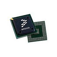
MPC5125YVN400 Freescale Semiconductor, MPC5125YVN400 Datasheet - Page 150

MPC5125YVN400
Manufacturer Part Number
MPC5125YVN400
Description
IC MCU 32BIT E300 324TEPBGA
Manufacturer
Freescale Semiconductor
Series
MPC51xxr
Datasheets
1.MPC5125YVN400.pdf
(92 pages)
2.MPC5125YVN400.pdf
(8 pages)
3.MPC5125YVN400.pdf
(2 pages)
4.MPC5125YVN400.pdf
(1064 pages)
Specifications of MPC5125YVN400
Core Processor
e300
Core Size
32-Bit
Speed
400MHz
Connectivity
CAN, EBI/EMI, Ethernet, I²C, USB OTG
Peripherals
DMA, WDT
Number Of I /o
64
Program Memory Type
ROMless
Ram Size
32K x 8
Voltage - Supply (vcc/vdd)
1.33 V ~ 1.47 V
Oscillator Type
External
Operating Temperature
-40°C ~ 125°C
Package / Case
324-PBGA
Processor Series
MPC51xx
Core
e300
Data Bus Width
32 bit
Development Tools By Supplier
TWR-MPC5125-KIT, TWR-SER, TWR-ELEV, TOWER
Maximum Clock Frequency
400 MHz
Operating Supply Voltage
1.4 V
Maximum Operating Temperature
+ 125 C
Mounting Style
SMD/SMT
Data Ram Size
32 KB
I/o Voltage
3.3 V
Interface Type
CAN, I2C
Minimum Operating Temperature
- 40 C
Program Memory Size
32 bit
Cpu Speed
400MHz
Embedded Interface Type
CAN, I2C, SPI, UART, USB
Digital Ic Case Style
TEPBGA
No. Of Pins
324
Rohs Compliant
Yes
Cpu Family
MPC5xx
Device Core Size
32b
Frequency (max)
400MHz
Total Internal Ram Size
32KB
Instruction Set Architecture
RISC
Operating Temp Range
-40C to 85C
Operating Temperature Classification
Industrial
Mounting
Surface Mount
Pin Count
324
Lead Free Status / RoHS Status
Lead free / RoHS Compliant
Eeprom Size
-
Program Memory Size
-
Data Converters
-
Lead Free Status / Rohs Status
Lead free / RoHS Compliant
Available stocks
Company
Part Number
Manufacturer
Quantity
Price
Company:
Part Number:
MPC5125YVN400
Manufacturer:
Freescale Semiconductor
Quantity:
135
Company:
Part Number:
MPC5125YVN400
Manufacturer:
LTC
Quantity:
29
Company:
Part Number:
MPC5125YVN400
Manufacturer:
Freescale Semiconductor
Quantity:
10 000
- MPC5125YVN400 PDF datasheet
- MPC5125YVN400 PDF datasheet #2
- MPC5125YVN400 PDF datasheet #3
- MPC5125YVN400 PDF datasheet #4
- Current page: 150 of 1064
- Download datasheet (6Mb)
Byte Data Link Controller (BDLC)
The receive shadow register works similarly. Once a complete byte has been received, the receive shift
register stores the newly received byte into the receive shadow register. The RDRF flag (or RXIFR flag if
the received byte is part of an IFR) is set to indicate that a new byte of data has been received. The
programmer has one BDLC module byte reception time to read the shadow register and clear the RDRF
or RXIFR flag before the shadow register is overwritten by the newly received byte.
If the user writes the first byte of a message to be transmitted to the BDLC Data Register and then
determines that a different message should be transmitted, the user can write a new byte to the BDLC Data
Register up until the transmission begins. This new byte replaces the original byte in the BDLC Data
Register.
From the time a byte is written to the BDLC Data Register until it is transferred to the transmit shift
register, the transmit shadow register is considered full and the byte pending transmission. If one of the
IFR transmission control bits (TSIFR, TMIFR1, or TMIFR0 in BDLC Control Register 2) is also set, the
byte is pending transmission as an IFR. A byte pending transmission is flushed from the transmit shadow
register and the transmission canceled if one of the following occurs: a loss of arbitration or transmitter
error on the byte currently being transmitted; a symbol error, framing error, bus fault, or BREAK symbol
is received. If the byte pending transmission is an IFR byte, the reception of a message with a CRC error
also causes the byte in the transmit shadow register to be flushed.
To abort an in-progress transmission, the programmer should simply stop loading more data into the
BDLC Data Register. This causes a transmitter underrun error and the BDLC module automatically
disables the transmitter on the next non-byte boundary. This means that the earliest a transmission can be
halted is after at least one byte (plus two extra 1-bits) has been transmitted. The receiver picks this up as
an error and relays it in the state vector register as an invalid symbol error.
6.3.2.5
The BDLC Analog Round Trip Delay Register (BDLC_DLCBARD) is used to program the BDLC
module so that it compensates for the round trip delays of different external transceivers. Also the polarity
of the receive pin (J1850_RX) is set in this register.
Read: any time
6-14
Address: Base + 0x05
D[7:0]
Reset
Field
W
R
BDLC Analog Round Trip Delay Register (BDLC_DLCBARD)
D7
Receive/Transmit Data
0
0
D6
1
0
Figure 6-6. BDLC Data Register (BDLC_DLCBDR)
MPC5125 Microcontroller Reference Manual, Rev. 2
Table 6-8. DLCBDR field descriptions
D5
0
2
D4
0
3
Description
D3
0
4
D2
0
5
Freescale Semiconductor
Access: User read/write
D1
0
6
D0
0
7
Related parts for MPC5125YVN400
Image
Part Number
Description
Manufacturer
Datasheet
Request
R
Part Number:
Description:
Mpc5125 Microcontroller Data Sheet
Manufacturer:
Freescale Semiconductor, Inc
Datasheet:

Part Number:
Description:
MPC5125 Microcontroller Data Sheet
Manufacturer:
FREESCALE [Freescale Semiconductor, Inc]
Datasheet:
Part Number:
Description:
Manufacturer:
Freescale Semiconductor, Inc
Datasheet:
Part Number:
Description:
Manufacturer:
Freescale Semiconductor, Inc
Datasheet:
Part Number:
Description:
Manufacturer:
Freescale Semiconductor, Inc
Datasheet:
Part Number:
Description:
Manufacturer:
Freescale Semiconductor, Inc
Datasheet:
Part Number:
Description:
Manufacturer:
Freescale Semiconductor, Inc
Datasheet:
Part Number:
Description:
Manufacturer:
Freescale Semiconductor, Inc
Datasheet:
Part Number:
Description:
Manufacturer:
Freescale Semiconductor, Inc
Datasheet:
Part Number:
Description:
Manufacturer:
Freescale Semiconductor, Inc
Datasheet:
Part Number:
Description:
Manufacturer:
Freescale Semiconductor, Inc
Datasheet:
Part Number:
Description:
Manufacturer:
Freescale Semiconductor, Inc
Datasheet:
Part Number:
Description:
Manufacturer:
Freescale Semiconductor, Inc
Datasheet:
Part Number:
Description:
Manufacturer:
Freescale Semiconductor, Inc
Datasheet:
Part Number:
Description:
Manufacturer:
Freescale Semiconductor, Inc
Datasheet:


