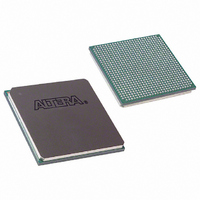
EP1S20F780I6N Altera, EP1S20F780I6N Datasheet - Page 324

EP1S20F780I6N
Manufacturer Part Number
EP1S20F780I6N
Description
IC STRATIX FPGA 20K LE 780-FBGA
Manufacturer
Altera
Series
Stratix®r
Specifications of EP1S20F780I6N
Number Of Logic Elements/cells
18460
Number Of Labs/clbs
1846
Total Ram Bits
1669248
Number Of I /o
586
Voltage - Supply
1.425 V ~ 1.575 V
Mounting Type
Surface Mount
Operating Temperature
-40°C ~ 100°C
Package / Case
780-FBGA
Family Name
Stratix
Number Of Logic Blocks/elements
18460
# I/os (max)
586
Frequency (max)
450.05MHz
Process Technology
0.13um (CMOS)
Operating Supply Voltage (typ)
1.5V
Logic Cells
18460
Ram Bits
1669248
Operating Supply Voltage (min)
1.425V
Operating Supply Voltage (max)
1.575V
Operating Temp Range
-40C to 100C
Operating Temperature Classification
Industrial
Mounting
Surface Mount
Pin Count
780
Package Type
FC-FBGA
Lead Free Status / RoHS Status
Lead free / RoHS Compliant
Number Of Gates
-
Lead Free Status / Rohs Status
Compliant
Available stocks
Company
Part Number
Manufacturer
Quantity
Price
Company:
Part Number:
EP1S20F780I6N
Manufacturer:
ALTERA
Quantity:
3 000
- Current page: 324 of 864
- Download datasheet (11Mb)
Enhanced PLLs
1–14
Stratix Device Handbook, Volume 2
Stratix and Stratix GX devices can drive any enhanced PLL driven
through the global clock or regional clock network to any general I/O pin
as an external output clock. The jitter on the output clock is not
guaranteed for these cases.
Clock Feedback
The following three feedback modes in Stratix and Stratix GX device
enhanced PLLs allow multiplication and/or phase shifting:
■
■
■
■
Table 1–7
Phase Shifting
Stratix and Stratix GX device enhanced PLLs provide advanced
programmable phase shifting. You set these parameters in the Quartus II
software.
No compensation mode
Normal Mode
Zero delay buffer mode
External feedback mode
Table 1–7. Clock Feedback Mode Availability
Clock Feedback Mode
Zero delay buffer: The external clock output pin is phase-aligned
with the clock input pin for zero delay. Altera recommends using the
same I/O standard on the input clock and the output clocks for
optimum performance.
External feedback: The external feedback input pin, FBIN, is phase-
aligned with the clock input, CLK, pin. Aligning these clocks allows
you to remove clock delay and skew between devices. This mode is
only possible for PLLs 5 and 6. PLLs 5 and 6 each support feedback
for one of the dedicated external outputs, either one single-ended or
one differential pair. In this mode, one encounter feeds back to the
PLL FBIN input, becoming part of the feedback loop.
Normal mode: If an internal clock is used in this mode, it is phase-
aligned to the input clock pin. The external clock output pin has a
phase delay relative to the clock input pin if connected in this mode.
No compensation: In this mode, the PLL does not compensate for
any clock networks or external clock outputs.
shows which modes are supported by which PLL type.
Enhanced PLLs
Yes
Yes
Yes
Yes
Mode Available in
Altera Corporation
Fast PLLs
Yes
Yes
No
No
July 2005
Related parts for EP1S20F780I6N
Image
Part Number
Description
Manufacturer
Datasheet
Request
R

Part Number:
Description:
CYCLONE II STARTER KIT EP2C20N
Manufacturer:
Altera
Datasheet:

Part Number:
Description:
CPLD, EP610 Family, ECMOS Process, 300 Gates, 16 Macro Cells, 16 Reg., 16 User I/Os, 5V Supply, 35 Speed Grade, 24DIP
Manufacturer:
Altera Corporation
Datasheet:

Part Number:
Description:
CPLD, EP610 Family, ECMOS Process, 300 Gates, 16 Macro Cells, 16 Reg., 16 User I/Os, 5V Supply, 15 Speed Grade, 24DIP
Manufacturer:
Altera Corporation
Datasheet:

Part Number:
Description:
Manufacturer:
Altera Corporation
Datasheet:

Part Number:
Description:
CPLD, EP610 Family, ECMOS Process, 300 Gates, 16 Macro Cells, 16 Reg., 16 User I/Os, 5V Supply, 30 Speed Grade, 24DIP
Manufacturer:
Altera Corporation
Datasheet:

Part Number:
Description:
High-performance, low-power erasable programmable logic devices with 8 macrocells, 10ns
Manufacturer:
Altera Corporation
Datasheet:

Part Number:
Description:
High-performance, low-power erasable programmable logic devices with 8 macrocells, 7ns
Manufacturer:
Altera Corporation
Datasheet:

Part Number:
Description:
Classic EPLD
Manufacturer:
Altera Corporation
Datasheet:

Part Number:
Description:
High-performance, low-power erasable programmable logic devices with 8 macrocells, 10ns
Manufacturer:
Altera Corporation
Datasheet:

Part Number:
Description:
Manufacturer:
Altera Corporation
Datasheet:

Part Number:
Description:
Manufacturer:
Altera Corporation
Datasheet:

Part Number:
Description:
Manufacturer:
Altera Corporation
Datasheet:

Part Number:
Description:
CPLD, EP610 Family, ECMOS Process, 300 Gates, 16 Macro Cells, 16 Reg., 16 User I/Os, 5V Supply, 25 Speed Grade, 24DIP
Manufacturer:
Altera Corporation
Datasheet:


