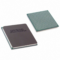
EP1S20F780I6N Altera, EP1S20F780I6N Datasheet - Page 453

EP1S20F780I6N
Manufacturer Part Number
EP1S20F780I6N
Description
IC STRATIX FPGA 20K LE 780-FBGA
Manufacturer
Altera
Series
Stratix®r
Specifications of EP1S20F780I6N
Number Of Logic Elements/cells
18460
Number Of Labs/clbs
1846
Total Ram Bits
1669248
Number Of I /o
586
Voltage - Supply
1.425 V ~ 1.575 V
Mounting Type
Surface Mount
Operating Temperature
-40°C ~ 100°C
Package / Case
780-FBGA
Family Name
Stratix
Number Of Logic Blocks/elements
18460
# I/os (max)
586
Frequency (max)
450.05MHz
Process Technology
0.13um (CMOS)
Operating Supply Voltage (typ)
1.5V
Logic Cells
18460
Ram Bits
1669248
Operating Supply Voltage (min)
1.425V
Operating Supply Voltage (max)
1.575V
Operating Temp Range
-40C to 100C
Operating Temperature Classification
Industrial
Mounting
Surface Mount
Pin Count
780
Package Type
FC-FBGA
Lead Free Status / RoHS Status
Lead free / RoHS Compliant
Number Of Gates
-
Lead Free Status / Rohs Status
Compliant
Available stocks
Company
Part Number
Manufacturer
Quantity
Price
Company:
Part Number:
EP1S20F780I6N
Manufacturer:
ALTERA
Quantity:
3 000
- Current page: 453 of 864
- Download datasheet (11Mb)
Altera Corporation
June 2006
An I/O bank featuring single-ended or differential standards can support
voltage-referenced standards as long as all voltage-referenced standards
use the same V
implement both SSTL-3 and SSTL-2 I/O standards, I/O pins using these
standards must be in different banks since they require different V
values
For voltage-referenced inputs, the receiver compares the input voltage to
the voltage reference and does not take into account the V
Therefore, the V
Voltage-referenced bidirectional and output signals must be the same as
the I/O bank’s V
SSTL-2 input pin in any I/O bank with a 1.25-V V
place SSTL-2 output pins in an I/O bank with a 2.5-V V
Mixing Voltage Referenced & Non-Voltage Referenced
Standards
Non-voltage referenced and voltage referenced pins can safely be mixed
in a bank by applying each of the rule-sets individually. For example, on
I/O bank can support SSTL-3 inputs and 1.8-V LVCMOS inputs and
outputs with a 1.8-V V
support 1.5-V LVCMOS, 3.3-V LVTTL (inputs, but not outputs), and
HSTL I/O standards with a 1.5-V V
For the voltage-referenced examples, see the
Guidelines”
I/O standards, see the
section. For details on how the Quartus II software supports
REF
CCIO
CCIO
setting. For example, although one I/O bank can
Selectable I/O Standards in Stratix & Stratix GX Devices
setting is irrelevant for voltage referenced inputs.
voltage. For example, although you can place an
CCIO
“Quartus II Software
and a 1.5-V V
CCIO
Stratix Device Handbook, Volume 2
and 0.75-V V
REF
. Similarly, an I/O bank can
Support”section.
“I/O Pad Placement
REF
level, you can only
REF
CCIO
.
CCIO
.
setting.
REF
4–25
Related parts for EP1S20F780I6N
Image
Part Number
Description
Manufacturer
Datasheet
Request
R

Part Number:
Description:
CYCLONE II STARTER KIT EP2C20N
Manufacturer:
Altera
Datasheet:

Part Number:
Description:
CPLD, EP610 Family, ECMOS Process, 300 Gates, 16 Macro Cells, 16 Reg., 16 User I/Os, 5V Supply, 35 Speed Grade, 24DIP
Manufacturer:
Altera Corporation
Datasheet:

Part Number:
Description:
CPLD, EP610 Family, ECMOS Process, 300 Gates, 16 Macro Cells, 16 Reg., 16 User I/Os, 5V Supply, 15 Speed Grade, 24DIP
Manufacturer:
Altera Corporation
Datasheet:

Part Number:
Description:
Manufacturer:
Altera Corporation
Datasheet:

Part Number:
Description:
CPLD, EP610 Family, ECMOS Process, 300 Gates, 16 Macro Cells, 16 Reg., 16 User I/Os, 5V Supply, 30 Speed Grade, 24DIP
Manufacturer:
Altera Corporation
Datasheet:

Part Number:
Description:
High-performance, low-power erasable programmable logic devices with 8 macrocells, 10ns
Manufacturer:
Altera Corporation
Datasheet:

Part Number:
Description:
High-performance, low-power erasable programmable logic devices with 8 macrocells, 7ns
Manufacturer:
Altera Corporation
Datasheet:

Part Number:
Description:
Classic EPLD
Manufacturer:
Altera Corporation
Datasheet:

Part Number:
Description:
High-performance, low-power erasable programmable logic devices with 8 macrocells, 10ns
Manufacturer:
Altera Corporation
Datasheet:

Part Number:
Description:
Manufacturer:
Altera Corporation
Datasheet:

Part Number:
Description:
Manufacturer:
Altera Corporation
Datasheet:

Part Number:
Description:
Manufacturer:
Altera Corporation
Datasheet:

Part Number:
Description:
CPLD, EP610 Family, ECMOS Process, 300 Gates, 16 Macro Cells, 16 Reg., 16 User I/Os, 5V Supply, 25 Speed Grade, 24DIP
Manufacturer:
Altera Corporation
Datasheet:


